Check patentability & draft patents in minutes with Patsnap Eureka AI!

Semiconductor device and method of controlling semiconductor device

Active Publication Date: 2012-08-02
RENESAS ELECTRONICS CORP
View PDF4 Cites 18 Cited by
  • Summary
  • Abstract
  • Description
  • Claims
  • Application Information

AI Technical Summary

Benefits of technology

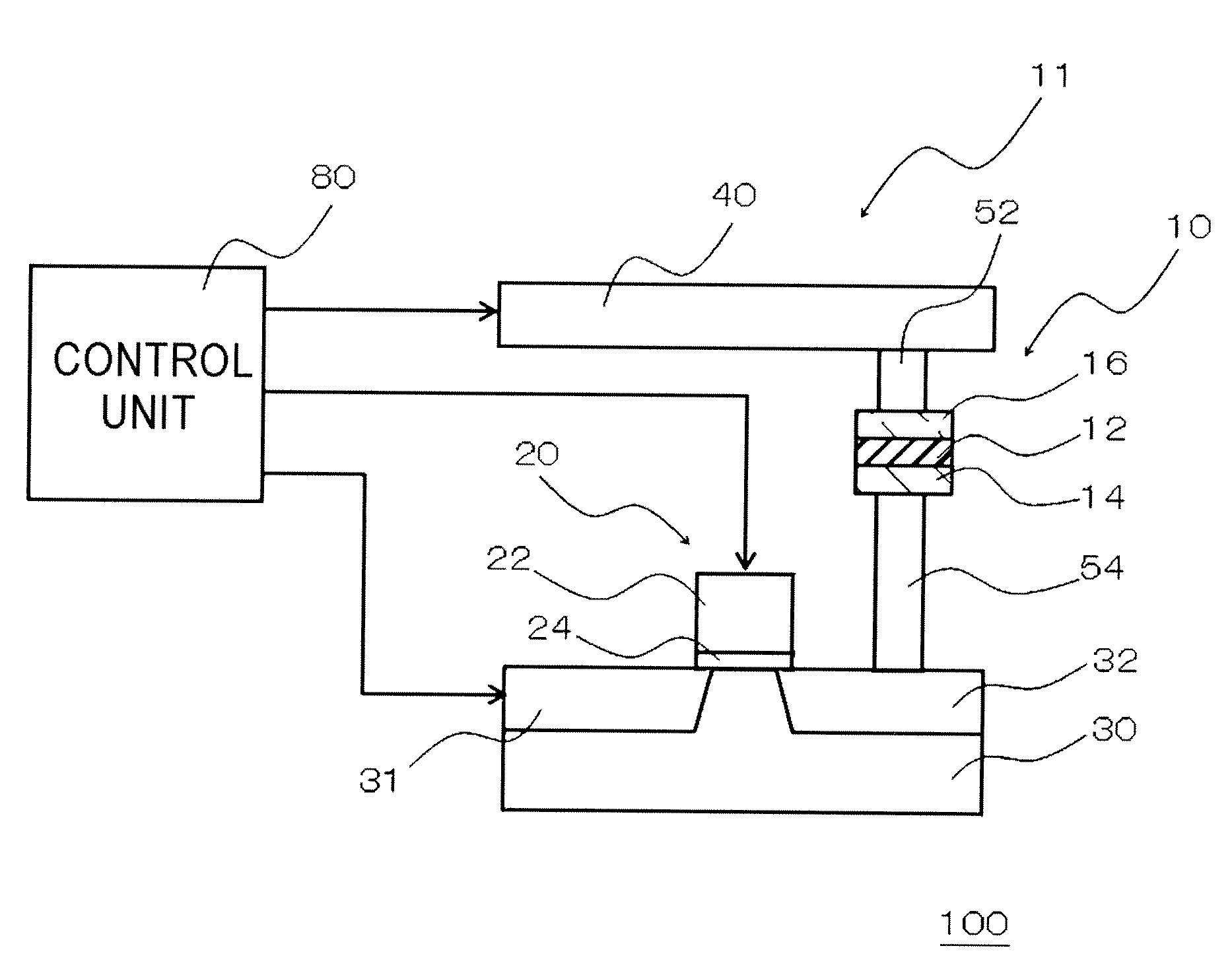
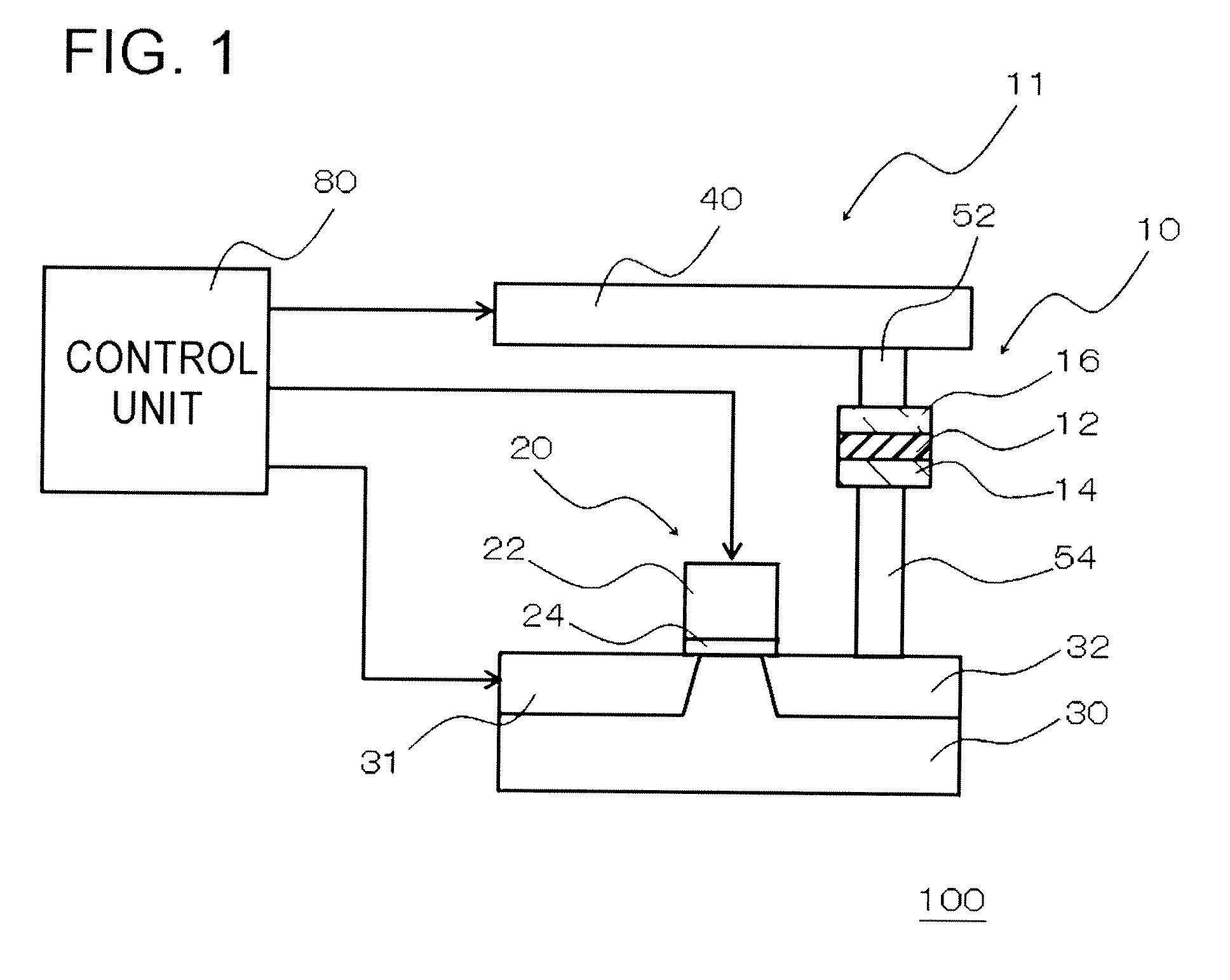
[0015]According to the invention, the first metal material constituting the first electrode has a normalized oxide formation energy higher than that of the second metal material constituting the second electrode. For this reason, even when a positive voltage is applied to the first electrode, the resistance state of the insulating film does not change into a high-resistance state. The control unit applies a positive voltage to the second electrode at the time of the operation of increasing the resistance value of the insulating film and the operation of decreasing the resistance value thereof, and applies a positive voltage to the first electrode at the time of the operation of reading out the resistance value of the insulating film. Therefore, it is possible to suppress the transition of the resistance state of the insulating film to a high-resistance state at the time of the readout operation. In addition, it is possible to perform the readout operation by a sufficiently high voltage. Consequently, it is possible to provide a semiconductor device capable of realizing the high-speed operation while assuring the reliability.
[0016]In another embodiment, a method is provided to control a semiconductor device including a first electrode containing a first metal material, a second electrode containing a second metal material, and an insulating film, provided between the first electrode and the second electrode, that contains a third metal material and oxygen, the first metal material having a normalized oxide formation energy higher than that of the second metal material, the method including: applying a positive voltage to the second electrode at the time of an operation of increasing a resistance value of the insulating film and an operation of decreasing the resistance value thereof, and applying a positive voltage to the first electrode at the time of an operation of reading out the resistance value of the insulating film.
[0017]According to the invention, it is possible to provide a semiconductor device with the high-speed operation while assuring the reliability.

Problems solved by technology

Further, even when the absolute value of a voltage to be applied at the time of readout is set lower than the absolute value of a voltage at which the transition to a high-resistance state is performed, there is also a problem of long-term reliability that the transition of the resistance state occurs by applying a readout voltage for a long period of time.
However, as the voltage applied at the time of the readout operation becomes lower, it takes more time to complete the readout operation.
In this manner, in the unipolar type nonvolatile memory, it is difficult to realize the high-speed operation while assuring the reliability thereof.

Method used


Image

  • Semiconductor device and method of controlling semiconductor device
  • Semiconductor device and method of controlling semiconductor device
  • Semiconductor device and method of controlling semiconductor device

Examples


example 1

[0368]FIG. 16 is a graph illustrating operation behavior of the nonvolatile memory 100 according to Example 1. In Example 1, a voltage was applied to the variable resistance device 10 obtained by laminating Ru (ΔHf=152.5 kJ / mol), TiO2 (ΔHf=472.5 kJ / mol), Ta2O5 (ΔHf=409.2 kJ / mol), and W (ΔHf=280.9667 to 294.85 kJ / mol) in this order, to examine the operation behavior of the nonvolatile memory 100. In this case, W constitutes the first electrode in the variable resistance device 10, and Ru constitutes the second electrode in the variable resistance device 10.

[0369]Meanwhile, FIG. 16 shows a relationship between the value of the voltage applied to the second electrode and the value of the current flowing to the variable resistance device 10. Hereinafter, the same is of FIG. 17 to 21.

[0370]As shown in FIG. 16, in Example 1, when a positive voltage was applied to the second electrode, the transition to a high-resistance state (OFF state) and the transition to a low-resistance state (ON st...

example 2

[0371]FIG. 17 is a graph illustrating operation behavior of the nonvolatile memory 100 according to Example 2. In Example 2, a voltage was applied to the variable resistance device 10 obtained by laminating Ru (ΔHf=152.5 kJ / mol), TiO2 (ΔHf=472.5 kJ / mol), Ta2O5 (ΔHf=409.2 kJ / mol), and TiN (ΔHf=303.5 kJ / mol) in this order, to examine the operation behavior of the nonvolatile memory 100. In this case, TiN constitutes the first electrode, and Ru constitutes the second electrode.

[0372]As shown in FIG. 17, in Example 2, when a positive voltage was applied to the second electrode, the transition to a high-resistance state (OFF state) and the transition to a low-resistance state (ON state) occurred. On the other hand, when a positive voltage was applied to the first electrode (a negative voltage was applied to the second electrode), the transition to a high-resistance state did not occur.

example 3

[0373]FIG. 18 is a graph illustrating operation behavior of the nonvolatile memory 100 according to Example 3. In Example 3, a voltage was applied to the variable resistance device 10 obtained by laminating Ru (ΔHf=152.5 kJ / mol), TiO2 (ΔHf=472.5 kJ / mol), Ta2O5 (ΔHf=409.2 kJ / mol), TiO2, and W (ΔHf=280.9667 to 294.85 kJ / mol) in this order, to examine the operation behavior of the nonvolatile memory 100. In this case, W constitutes the first electrode, and Ru constitutes the second electrode.

[0374]As shown in FIG. 18, in Example 3, when a positive voltage was applied to the second electrode, the transition to a high-resistance state (OFF state) and the transition to a low-resistance state (ON state) occurred. On the other hand, when a positive voltage was applied to the first electrode (a negative voltage was applied to the second electrode), the transition to a high-resistance state did not occur.


PUM


Abstract

Provided is a semiconductor device including: a memory cell having a variable resistance device; and a control unit that controls a voltage applied to the memory cell, wherein the variable resistance device includes a lower electrode contains a first metal material, an upper electrode containing a second metal material, and an insulating film containing oxygen, the first metal material has a normalized oxide formation energy higher than that of the second metal material, and the control unit applies a positive voltage to the upper electrode at the time of an operation of increasing a resistance value of the insulating film and an operation of decreasing the resistance value thereof, and applies a positive voltage to the lower electrode at the time of an operation of reading out the resistance value of the insulating film.

Description

[0001]This application is based on Japanese patent application Nos. 2011-018703, 2011-125331, and 2011-237272, the contents of which are incorporated herein by reference.BACKGROUND[0002]1. Technical Field[0003]The present invention relates to a semiconductor device and a method of controlling a semiconductor device.[0004]2. Related Art[0005]A variable resistance storage device (ReRAM: Resistance Random Access Memory) is one type of nonvolatile memory which utilize a change of resistance value of an insulating film provided between electrodes by the application of a voltage. As operation types of ReRAM, there are a unipolar type and a bipolar type. In the unipolar type, any of the state transitions of an increase in the resistance of an insulating film and a decrease in the resistance thereof occurs due to the application of a voltage in the same direction. On the other hand, in the bipolar type, an increase in the resistance of an insulating film occurs due to the application of a v...

Claims


Application Information

Patent Timeline
IPC IPC(8): G11C11/00
CPCG11C13/0007H01L27/2436G11C13/004G11C13/0069G11C2013/0083G11C2013/009G11C2213/15G11C2213/54G11C2213/56G11C2213/74G11C2213/79G11C2213/82H01L27/101H01L45/145H01L45/04G11C13/003H10B63/30H10N70/20H10N70/883H10N70/8833
Inventor SAITOH, MOTOFUMITERAI, MASAYUKI
Owner RENESAS ELECTRONICS CORP
Features
  • R&D
  • Intellectual Property
  • Life Sciences
  • Materials
  • Tech Scout
  • Unparalleled Data Quality
  • Higher Quality Content
  • 60% Fewer Hallucinations
Learn More