

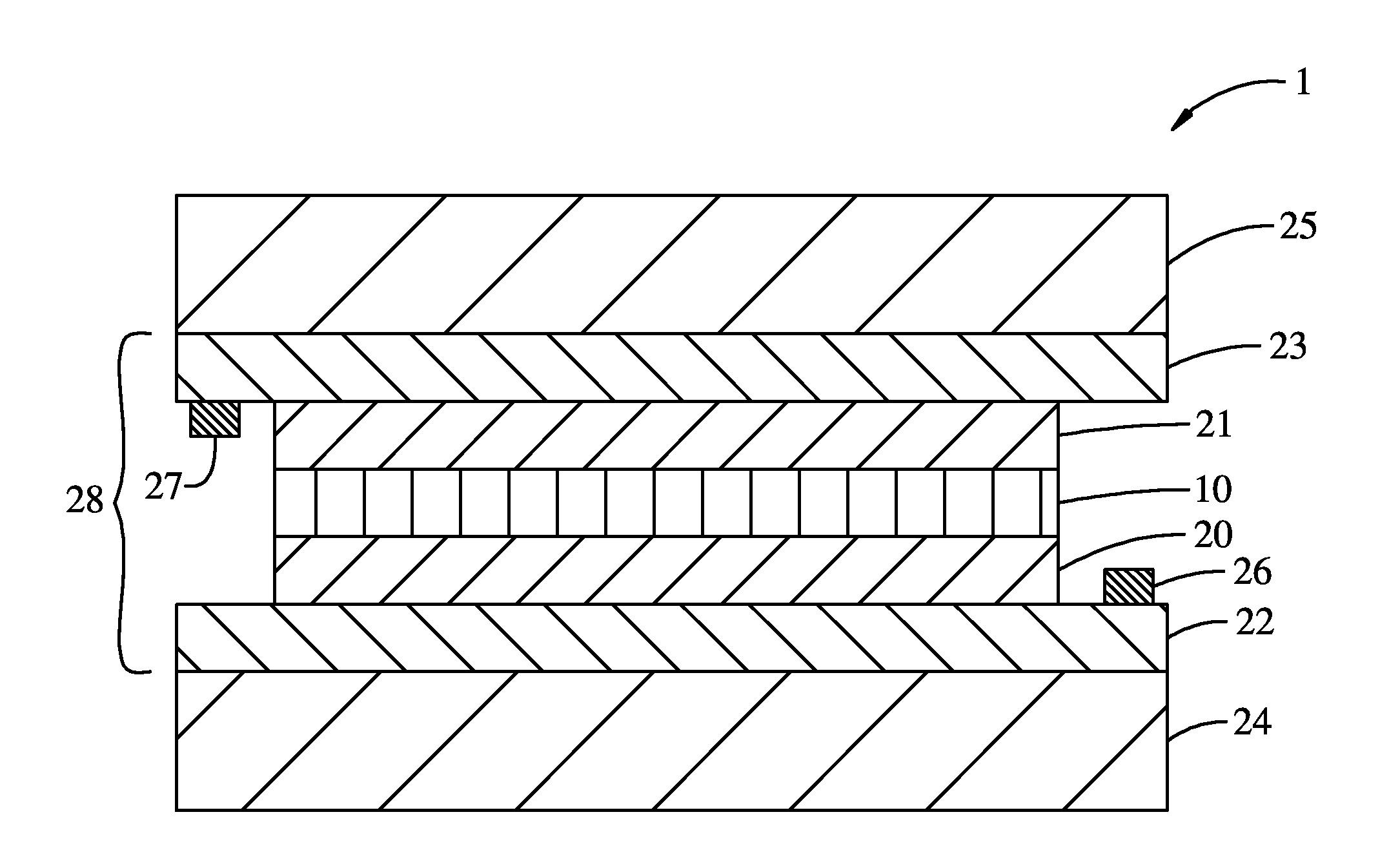
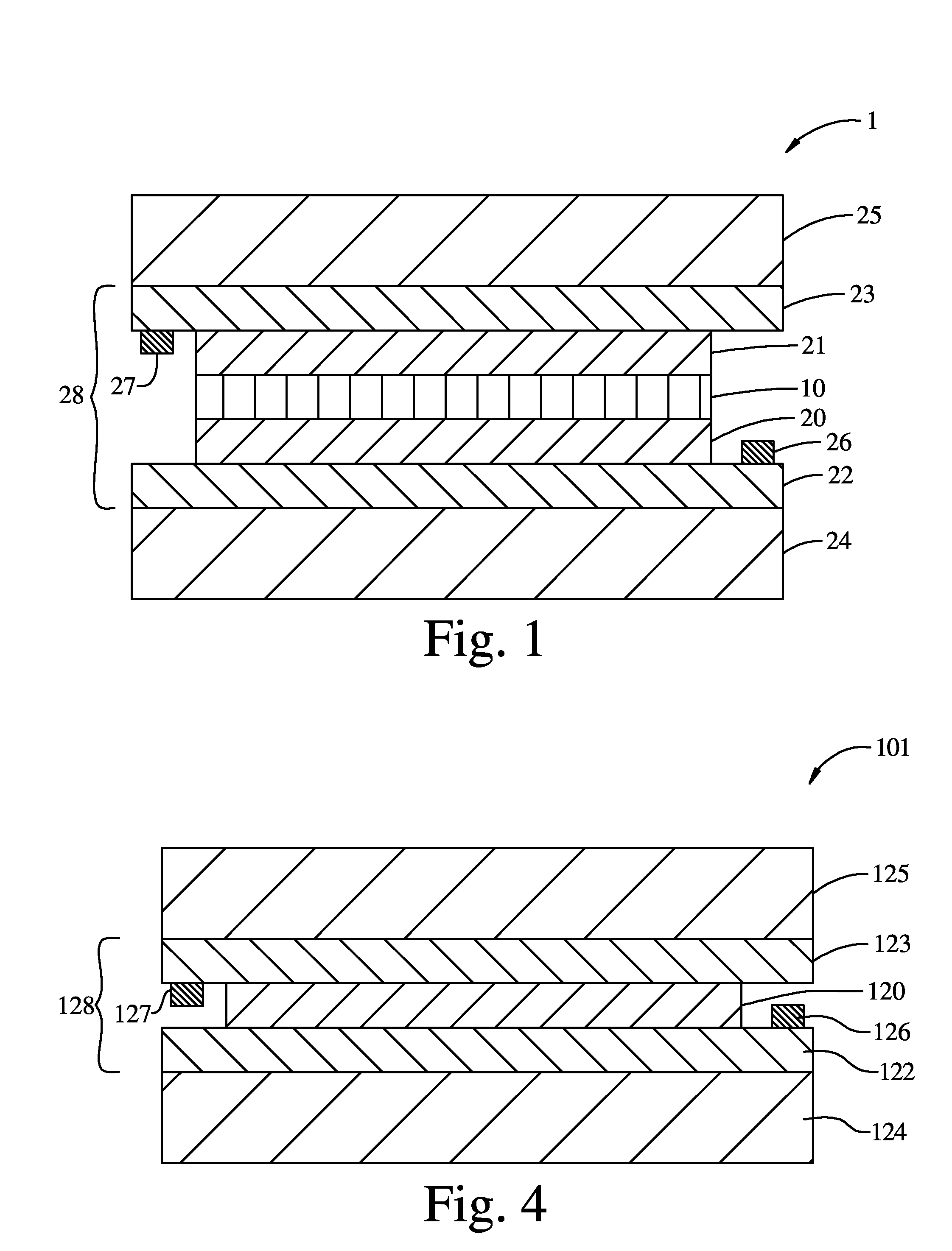
Electrochromic multi-layer devices with spatially coordinated switching
a multi-layer device and electrochromic technology, applied in the direction of liquid surface applicators, coatings, instruments, etc., can solve the problems of non-uniform coloring or switching, non-uniform switching, and significant difference between the transmissivity near the edge of the device and the transmissivity at the center of the device, so as to achieve the effect of convenient manufacturing
- Summary
- Abstract
- Description
- Claims
- Application Information
AI Technical Summary
Benefits of technology
Problems solved by technology
Method used
Image

Examples
example 1
Iris Effect Switching
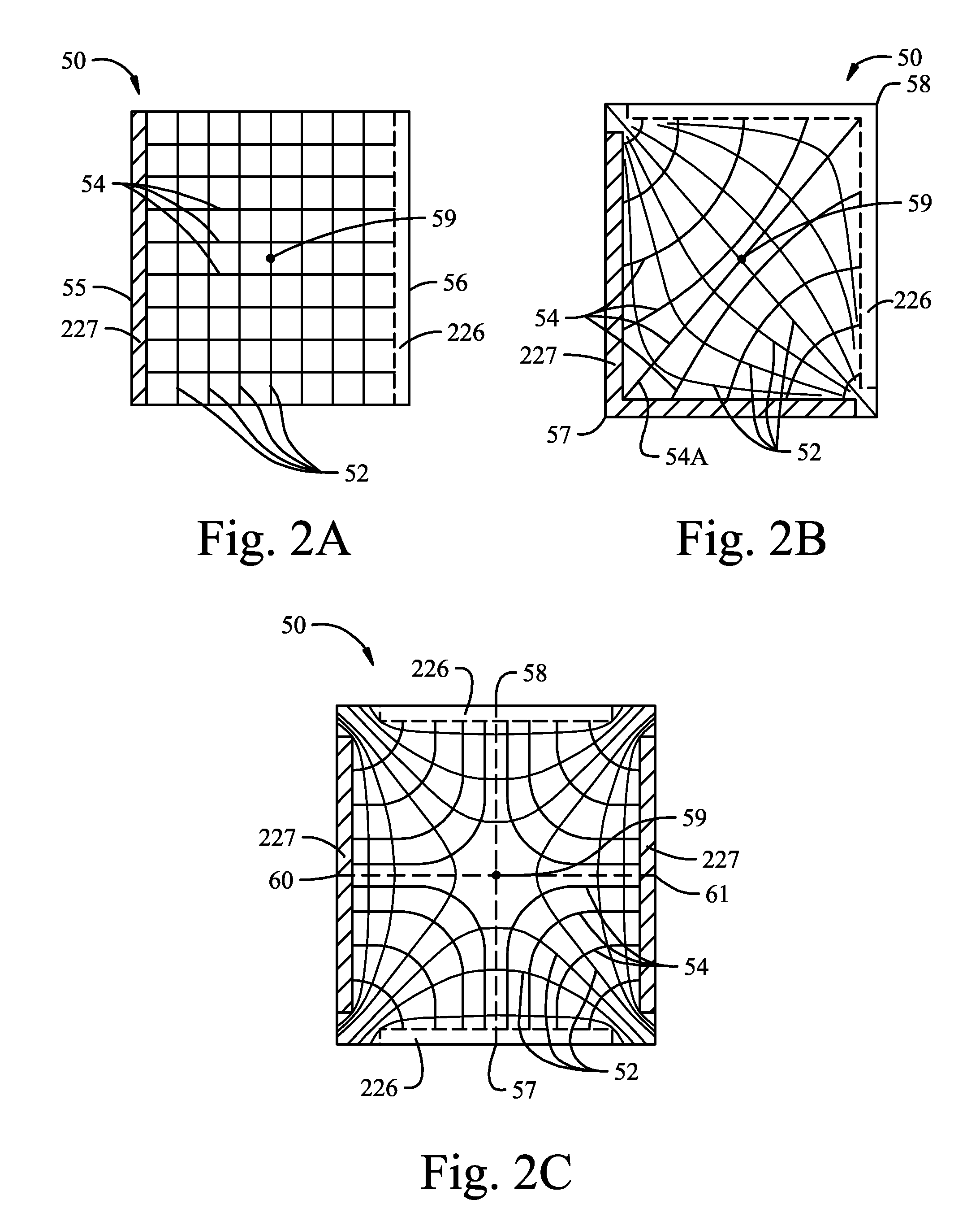
[0108]A 1-D lumped element circuit model has been used to simulate the dynamic behavior of an electrochromic type device using component values appropriate to capture the switching dynamics of a large area device. The lumped element model shown in FIG. 5 is based on a paper by Skrayabin et. al. (Electrochimica Acta 44 (1999) 3203-3209). The electrochromic device is locally modeled by a parallel resistor and non-linear capacitor and the electrically conducting layer is locally modeled as a resistor. A network of these devices as shown in FIG. 5 models the behavior of a large area electrochromic device. A low resistance resistor between the device and the power supply simulates the contact resistance between the power supply and the device. FIG. 6 shows the applied voltage, a 1.1 volt step function. The resultant current flow is shown in FIG. 7; it rises rapidly to a maximum value and then decreases as the device switching takes place. FIG. 8 shows the voltage dro...
example 2
Uniform Switching
[0110]The 1-D circuit model shown in FIG. 12 embodies a constant gradient in sheet resistance in each of the electrically conducting layers. These are arranged such that the sheet resistance is lowest near the connection the power supply and highest at the opposite end of the device. One polarity of the power supply is applied to one electrically conducting layer and the other polarity of the power supply is applied to the opposing electrically conducting layer and at the opposite sides of the device. With this arrangement there is no iris effect and switching behavior is qualitatively different—providing both uniform switching across the entire device and much faster switching of the entire device. This switching behavior is shown in FIGS. 13-15. FIG. 13 shows the applied voltage waveform. This waveform was selected to limit the voltage across the device to always be below a desired threshold (in this example 1.0 volts). The resultant waveform is a voltage pulse wi...
example 3
Directional Switching
[0111]The lumped element model in FIG. 16 is an example of a configuration that provides a controlled switching profile in an electrochromic device. In this case, the device will switch from left to right. The electrically conducting layers are asymmetric. The top electrically conducting layer is a layer with sheet resistance of 5Ω / □ at the left side and linearly increasing to 50Ω / □ at the right side of this layer. The bottom electrically conducting layer is a layer with sheet resistance of 30Ω / □ at the left side and linearly decreasing to 3Ω / □ at the right side of the layer. FIG. 17 shows the applied voltage waveform to product a rapidly rising voltage at the left side of the device while keeping this voltage across the device below 1.0 volts. FIG. 18 shows the corresponding current through the device which initially rapidly increases then quickly falls as the device switches. FIG. 19 shows the voltage across the device at six location from left to right. As ca...
PUM
| Property | Measurement | Unit |
|---|---|---|
| ionic conductivity | aaaaa | aaaaa |
| surface area | aaaaa | aaaaa |
| length | aaaaa | aaaaa |
Abstract
Description
Claims
Application Information