In-situ hydrogen plasma treatment of amorphous silicon intrinsic layers

Inactive Publication Date: 2012-08-09
APPLIED MATERIALS INC
View PDF4 Cites 7 Cited by
  • Summary
  • Abstract
  • Description
  • Claims
  • Application Information

AI Technical Summary

Benefits of technology

[0011]Embodiments of the invention generally provide methods for forming amorphous silicon-based photovoltaic (PV) devices, such as solar or PV cells, by utilizing deposition steps and plasma treatment steps during a plasma-enhanced chemical vapor deposition (PE-CVD) process. The amorphous silicon (α-Si) materials, layers, and films formed by utilizing processes described herein have less lattice defects and impurities relative to α-Si materials formed by previous deposition processes. Therefore, a PV device or cell containing the α-Si materials formed by processes described herein has less premature failure and maximizes

Problems solved by technology

Generally, PE-CVD processes provide increased deposition rates for α-Si materials but at a cost of increased defects in the silicon lattice relative to thermal CVD processes.
Similarly, defects in the silicon lattice are often formed upon plasma exposure of the α-Si material by any of a variety of plasma processes including post deposition plasma anneal step, a plasma cle

Method used


Image

  • In-situ hydrogen plasma treatment of amorphous silicon intrinsic layers
  • In-situ hydrogen plasma treatment of amorphous silicon intrinsic layers
  • In-situ hydrogen plasma treatment of amorphous silicon intrinsic layers

Examples


Example

[0026]Embodiments of the invention generally provide methods for forming amorphous silicon-based photovoltaic (PV) devices, such as solar or PV cells, by utilizing deposition steps and plasma treatment steps during a plasma-enhanced chemical vapor deposition (PE-CVD) process.

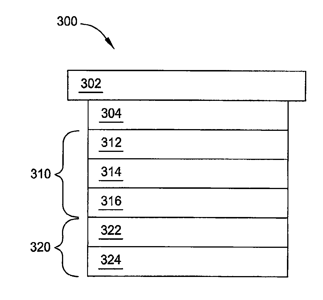
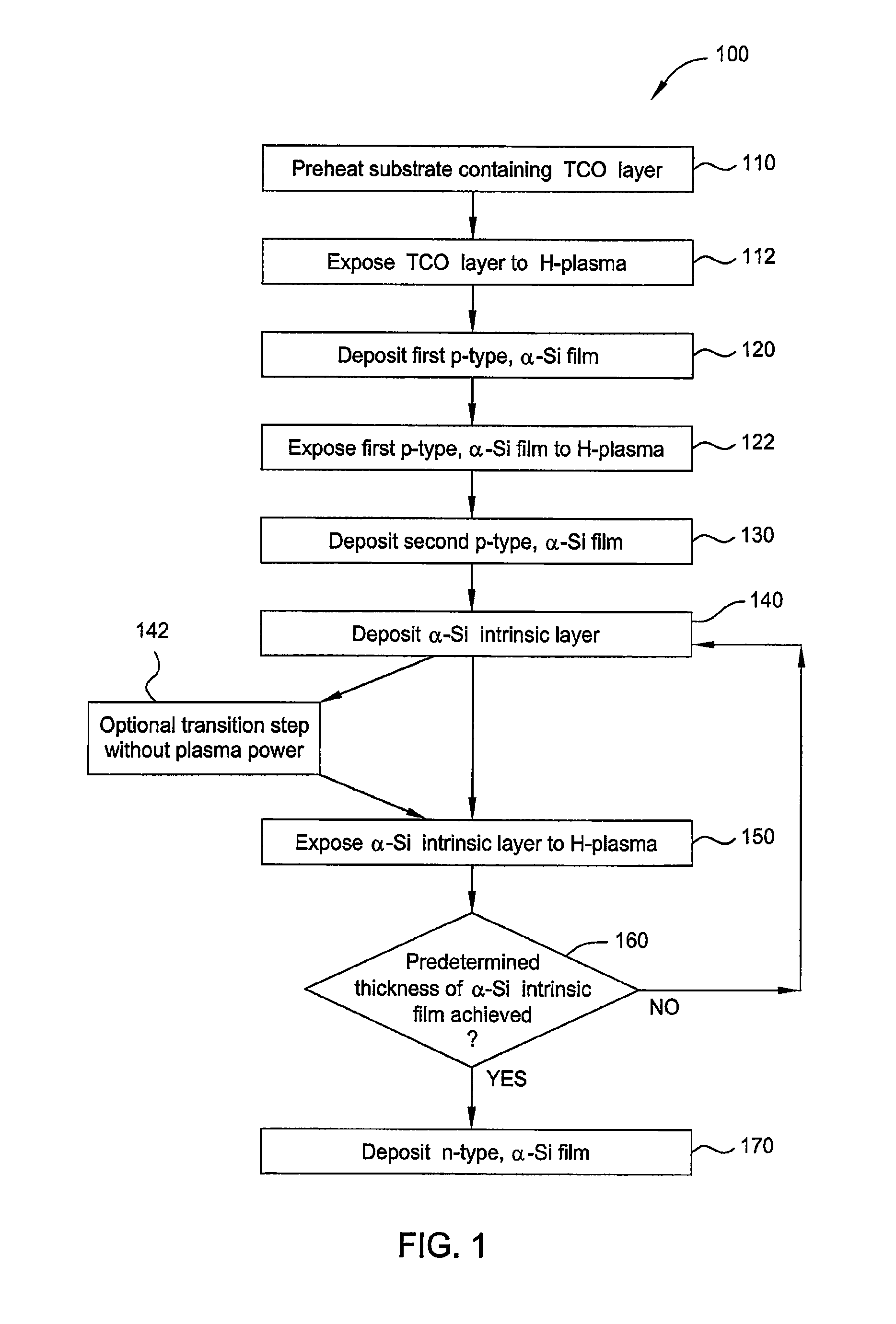
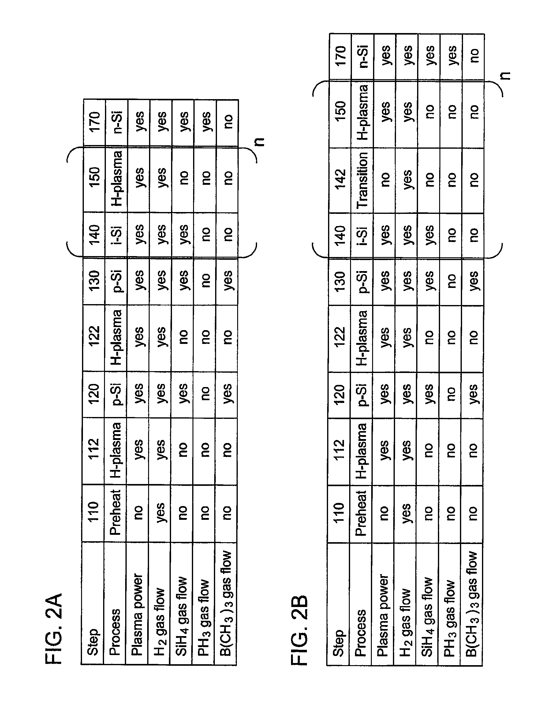
[0027]FIG. 1 shows a flow chart depicting process 100, which is utilized to form solar or PV devices or cells containing at least one amorphous silicon (α-Si) p-i-n junction, as described by embodiments herein. In one embodiment, process 100 includes the steps of preheating a substrate having a transparent conductive oxide (TCO) layer disposed thereon at step 110, exposing the TCO layer on the substrate to a hydrogen plasma at step 112, depositing or forming a first p-type, amorphous silicon (α-Si) film on or over the TCO layer at step 120, exposing the first p-type, α-Si film to the hydrogen plasma at step 122, and depositing a second p-type α-Si film on or over the first p-type, α-Si film at step 130.

[0028]Pro...


PUM


Abstract

Embodiments of the invention generally provide methods for forming amorphous silicon-based photovoltaic devices, such as solar cells, by utilizing deposition and plasma treatment steps during a plasma-enhanced chemical vapor deposition (PE-CVD) process. In one embodiments, the method includes exposing a transparent conductive oxide (TCO) layer disposed on a substrate to hydrogen plasma during pretreatment, forming a p-type α-Si film on the TCO layer, forming an α-Si intrinsic film on the p-type α-Si film during a PE-CVD process, and forming an n-type α-Si film on the α-Si intrinsic film. In some examples, the PE-CVD process includes depositing an α-Si intrinsic layer during a deposition step, treating the α-Si intrinsic layer to form a treated α-Si intrinsic layer during a plasma treatment step, and sequentially repeating the deposition step and the plasma treatment step until obtaining a desired thickness of the α-Si intrinsic film containing a plurality of treated α-Si intrinsic layers.

Description

CROSS-REFERENCE TO RELATED APPLICATION[0001]This application claims benefit of U.S. Ser. No. 61 / 439,190 (APPM / 015540L), filed Feb. 3, 2011, which is herein incorporated by reference in its entirety.BACKGROUND OF THE INVENTION[0002]1. Field of the Invention[0003]Embodiments of the invention generally relate to methods for forming photovoltaic devices, and more particularly to vapor deposition and plasma treatment processes utilized to form thin film photovoltaic devices.[0004]2. Description of the Related Art[0005]Solar or photovoltaic (PV) cells are devices which convert sunlight into direct current (DC) electrical power. Each individual PV cell generates a specific amount of electrical energy. Therefore, multiple PV cells may be bundled or tiled into a solar module that is scaled to deliver a desired amount of electrical energy.[0006]PV or solar cells typically have one or more p-i-n junctions. When the p-i-n junction of the PV cell is exposed to photons, such as from sunlight, the...

Claims


Application Information

Patent Timeline
IPC IPC(8): H01L31/0264
CPCH01L31/03762Y02E10/548H01L31/202H01L31/075Y02P70/50
Inventor WHITESELL, III, HARRY SMITHALCOTT, GREGORY ROBERT
Owner APPLIED MATERIALS INC
Why Eureka
Try Eureka