Graphene-based thin films in heat circuits and methods of making the same

a graphene-based, heat-sealed film technology, applied in the direction of instruments, natural mineral layered products, synthetic resin layered products, etc., can solve the problems of limited radio frequency (rf) transparency, limited frequency operation band, numerous limitations of present-day heat-sealed circuits, etc., and achieve high conductive and low weight

Inactive Publication Date: 2012-08-16
RICE UNIV +1
View PDF5 Cites 36 Cited by
  • Summary
  • Abstract
  • Description
  • Claims
  • Application Information

AI Technical Summary

Benefits of technology

[0009]The methods and compositions of the present invention provide numerous applications and advantages. In some embodiments, the present invention provides thin and affordable heat circuits that are low in weight, highly conductive, and transparent. In various embodiments, the films of the present invention may be used as coatings for de-icing or anti-icing applications, including the de-icing of antennas, radomes, or aircraft structures such as wing edges.

Problems solved by technology

Present-day heat circuits have numerous limitations.
Such limitations include bulkiness, limited radio frequency (RF) transparency, restricted frequency operation band, high incretion loss, high sensitivity to RF signal polarization, restricted antenna beam scan performance, and high costs.

Method used


Image

  • Graphene-based thin films in heat circuits and methods of making the same
  • Graphene-based thin films in heat circuits and methods of making the same
  • Graphene-based thin films in heat circuits and methods of making the same

Examples


example 1

Fabrication of GNR Films

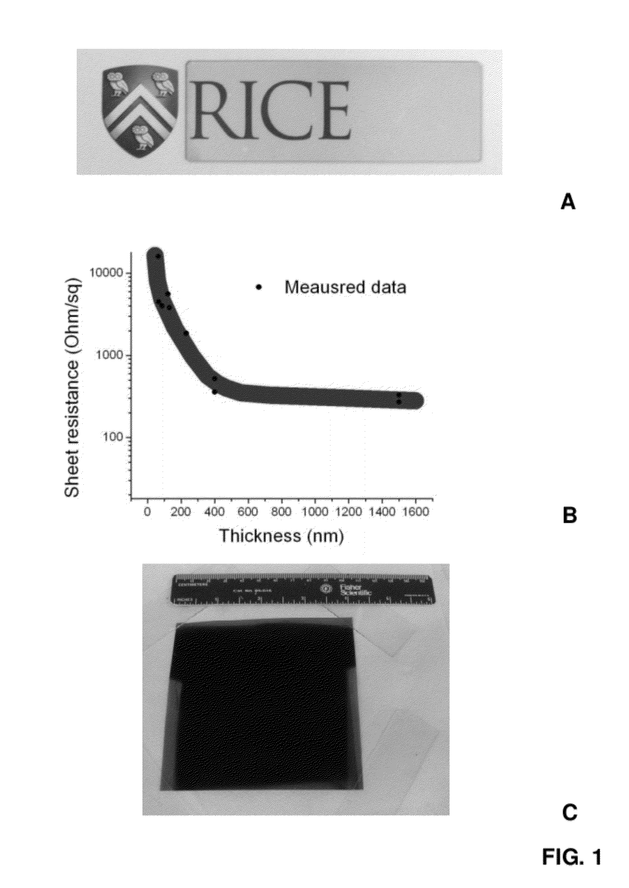
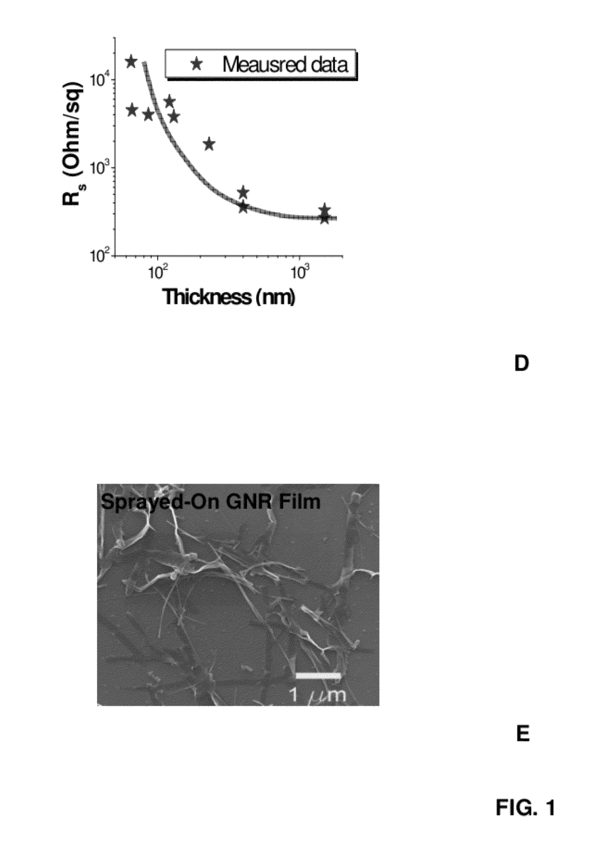
[0081]A typical fabrication procedure for a GNR film involves the steps described herein. First, a glass surface was cleaned with acetone and deionized water. Next, polyurethane (a type used a clear-coat automotive paint) was spin-coated on the glass surface. Typical spin times were about 60 seconds at around 4,000 rpm. The sample was then left at room temperature for 12 hours until the film was solidified. Next, the glass substrate with the polyurethane coating was placed on a hot plate at 200° C. A pre-made solution of GNRs dissolved in ortho-dichlorobenzene to a concentration of about 1 mg / mL was then sprayed onto the surface of the glass using an airbrush. The sample was then washed with ethanol to remove the residual solvent. In other embodiments, a polyimide film was used as a substrate. Photographs of the fabricated GNR films are shown in FIGS. 1A and 1C. The relationship between sheet resistance and GNR film thickness was also studied. See FIGS. 1B an...

example 2

Modeling RF Transmission Through GNR Films

[0083]The straightforward way to evaluate RF transmission through a thin conductive layer is based on a skin depth concept. The theory shows that an electromagnetic wave propagating inside the conductive material reduces in magnitude by factor 1 / e in a distance Δ(skin depth in meters), in accordance with the following formula:

Δ=503 / √{square root over (fμσ)}  (1),

where f is the frequency in Hz, μ is the relative magnetic permeability of conductive material, and σ is the bulk electrical conductance in S / m.

[0084]Since antenna and radome de-icing is considered as an application of this work, it is convenient to use frequencies in the GHz range. The isotropic GNR film is not magnetic. Thus, μ=1. At the GHz frequency range, the skin depth can be calculated by the following formula where m is meter:

Δ=0.016fσ[m](2)

[0085]The electrical field strength decreases exponentially at the distance d, in accordance with the following equation L:

E∼-dΔ=-63dfσ(3...

example 3

Properties of GNR Films

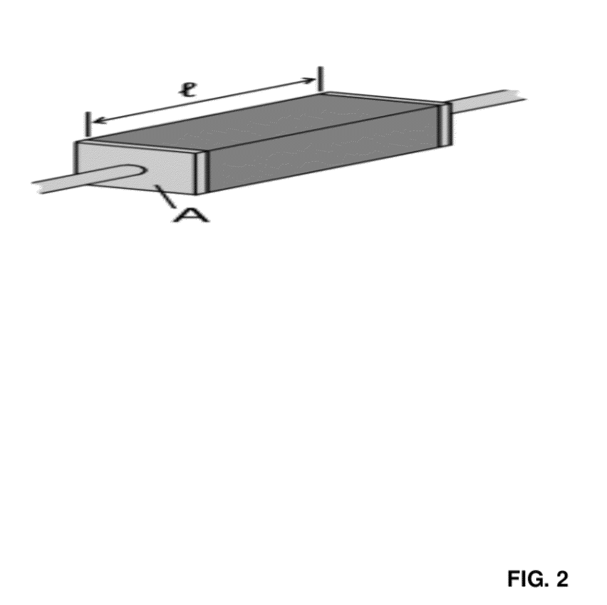
[0087]The conductivity and resistance of GNR films on polyimide substrates were studied. In these experiments, the GNR films were placed between copper electrodes, as illustrated in FIG. 2. Table 1 provides a summary of the obtained data.

TABLE 1Properties of GNR films on polyimide substrateswith a polyurethane adhesion layer.Resistance atGrapheneAmbientDC EffectiveGrapheneLayerSolutionTemperatureConductivitySkin DepthActive AreaThicknesssprayed(KΩ)(KS / m)Δ (nm)(inches)(nm)(mL)12.517.24~1.1 × 1051 × 2~1107.529.942.68  ~2 × 1051 × 2~755

[0088]The DC effective conductivity of the GNR films was calculated through the measured resistance as

σ=lA*R=2*109Rt[Sm],(4)

where A=w*t, w is the graphene layer width of 1 inch, t is graphene layer thickness, and l is the graphene layer length of 2 inch.

[0089]Another square sheet of a GNR film between copper electrodes is shown in FIG. 4A. In this example, the GNR film has a surface area of 1×1 meter square (˜40×40 inch=1600 square...


PUM

PropertyMeasurementUnit
thicknessaaaaaaaaaa
thicknessaaaaaaaaaa
temperatureaaaaaaaaaa

Abstract

In various embodiments, the present invention provides electrically conductive and radio frequency (RF) transparent films that include a graphene layer and a substrate associated with the graphene layer. In some embodiments, the graphene layer has a thickness of less than about 100 nm. In some embodiments, the graphene layer of the film is adhesively associated with the substrate. In more specific embodiments, the graphene layer includes graphene nanoribbons that are in a disordered network. Further embodiments of the present invention pertain to methods of making the aforementioned electrically conductive and RF transparent films. Such methods generally include associating a graphene composition with a substrate to form a graphene layer on a surface of the substrate.

Description

CROSS-REFERENCE TO RELATED APPLICATIONS[0001]This application claims priority to U.S. Provisional Patent Application No. 61 / 434,713, filed on Jan. 20, 2011. The entirety of the above-identified provisional application is incorporated herein by reference.STATEMENT REGARDING FEDERALLY SPONSORED RESEARCH[0002]This invention was made with government support under the Air Force Office of Scientific Research Grant No. FA9550-09-1-0581 and the Office of Naval Research Grant No. N000014-09-1-1066, both awarded by the U.S. Department of Defense. The government has certain rights in the invention.BACKGROUND OF THE INVENTION[0003]Present-day heat circuits have numerous limitations. Such limitations include bulkiness, limited radio frequency (RF) transparency, restricted frequency operation band, high incretion loss, high sensitivity to RF signal polarization, restricted antenna beam scan performance, and high costs. Therefore, a need exists for the development of improved heat circuits that ar...

Claims


Application Information

Patent Timeline
Patent Type & Authority Applications(United States)
IPC IPC(8): B32B9/00B32B13/04B32B27/40B32B17/06B32B27/38B82Y40/00B82Y99/00
CPCB82Y30/00B82Y40/00C01B31/0253Y10T428/265C01B31/0293C01B31/0484H01B1/04C01B31/0273C01B32/168C01B32/174C01B32/18C01B32/194Y10T428/31721Y10T428/31551Y10T428/31511Y10T428/31855
Inventor TOUR, JAMES M.VOLMAN, VLADIMIRZHU, YU
Owner RICE UNIV
Why Eureka
Try Eureka