Method and apparatus for forming silicon dots and method and apparatus for forming a substrate with silicon dots and insulating film
Inactive Publication Date: 2012-08-23
NISSIN ELECTRIC CO LTD
View PDF5 Cites 9 Cited by
Summary
Abstract
Description
Claims
Application Information
AI Technical Summary
This helps you quickly interpret patents by identifying the three key elements:
Problems solved by technology
Method used
Benefits of technology
Benefits of technology
[0106]As already mentioned, the present invention can provide a method and an apparatus for forming silicon dots which can form silicon dots at a relatively low temperature, suppress defects and clustering of silicon dots, which may be generated at a high temperature, and damages to silicon dots caused by plasma, and can further form silicon dots with high controllability of the particle diameter of the silicon dots, and with high reproducibility between substrates.
[0107]The present invention can also provide a method and an apparatus for forming a substrate with silicon dots and insulating film at a relatively low temperature, which can suppress defects and clustering of silicon dots, which may occur at a high temperature, and damages to silicon dots and insulating film caused by plasma, and further with high controllability of the particle diameter of the silicon dots and high controllability of the thickness of the insulating film, and with high reproducibility between substrates.
Problems solved by technology
However, there still remains some problems even if the plasma CVD method is employed so that silicon dots and insulating films can be formed even at a relatively low temperature; the inductively coupled plasma CVD method in which the antenna disposed in the plasma producing chamber is used is employed to improve the efficiency of utilization of the input power and for other purposes; and an antenna with reduced inductance is employed to produce high-density plasma and form desired silicon dots and insulating films while suppressing abnormal discharge from the internal antenna and protecting the to-be-processed substrate, the silicon dots formed thereon and the insulating film from damages by plasma.
Method used
Image
Click on the blue label to locate the original text in one second.
Reading with bidirectional positioning of images and text.
Examples
example 1
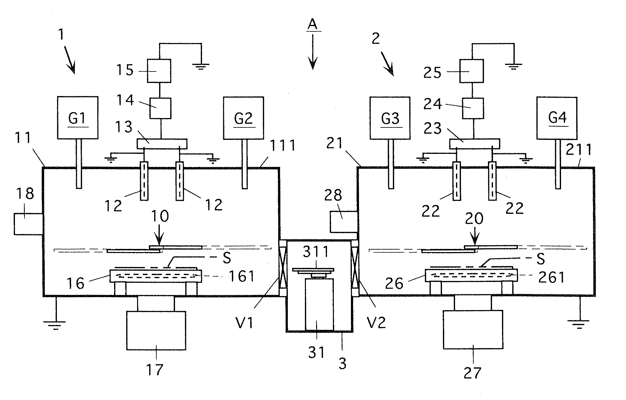
[0200](1) To begin with, the substrate S on which a tunnel silicon oxide film is formed by subjecting the surface of a P-type semiconductor silicon substrate as the to-be-processed substrate S to a thermal oxidation treatment in advance is supported on the substrate holder 16 in the plasma producing chamber 11, and the substrate is heated to 220° C. by the heater 161.
(2) The chamber 11 is evacuated by the exhaust device 17 to reduce the pressure inside the chamber 11 to 2×10⁻⁴ Pa or lower, and then monosilane (SiH4) gas (0.2 ccm) and hydrogen gas (30 ccm) are supplied into the chamber 11.
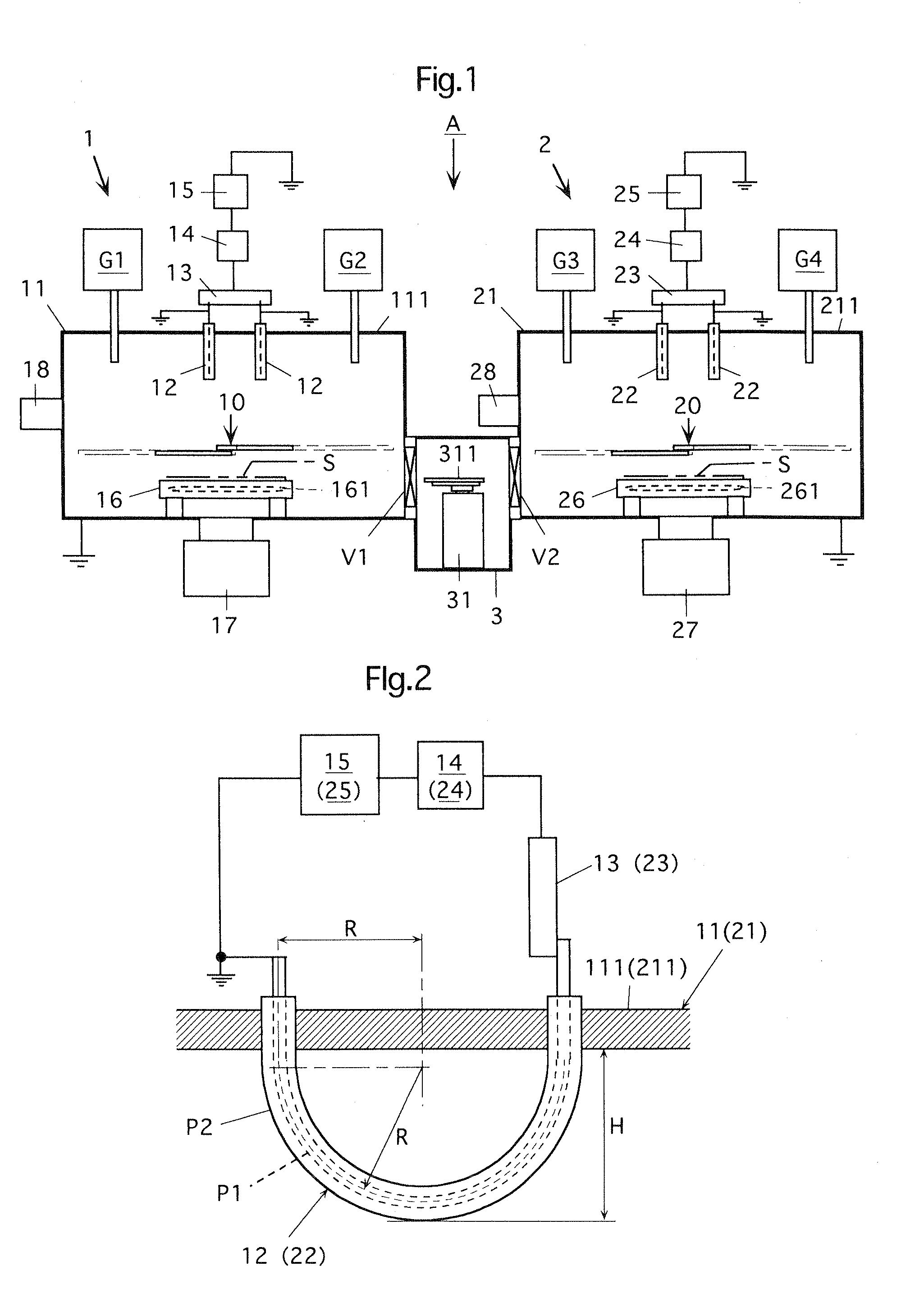
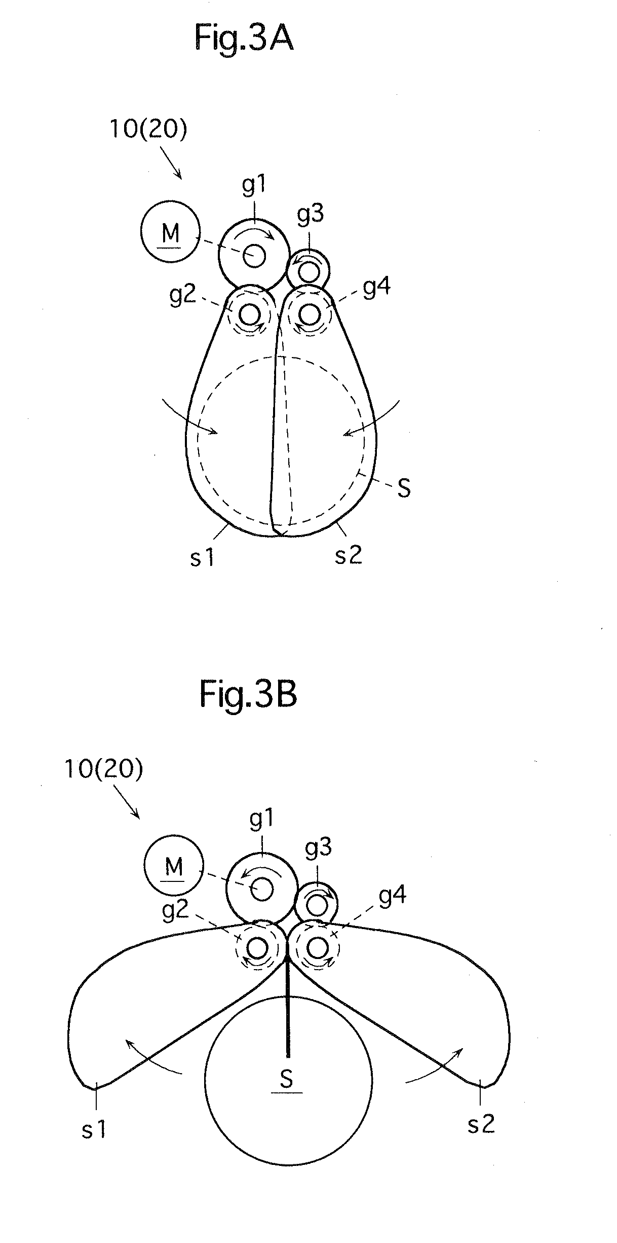
(3) While the pressure inside the chamber 11 is maintained to a silicon dot formation pressure of 0.8 Pa (6 mTorr) by supplying the gases and by the operation of the exhaust device 17, high-frequency power of 13.56 MHz and 2000 W is applied to the antennas 12 in a state that the shutter device 10 is closed to cover the substrate S, as shown in FIG. 5, so that formation of inductively coupled plasma ...
example 2
[0211](1) To begin with, the substrate S on which a tunnel silicon oxide film is formed by subjecting the surface of a P-type semiconductor silicon substrate as the to-be-processed substrate S to a thermal oxidation treatment in advance is supported on the substrate holder 19 in the plasma producing chamber 11, and the substrate is heated to 220° C.
(2) The gate valve V1 is opened to evacuate the chamber 11 and path 3′ by the exhaust device 17 and reduce the pressure inside the chamber 11 and path 3′ to 2×10⁻⁴ Pa or lower, and then monosilane (SiH4) gas (0.2 ccm) and hydrogen gas (30 ccm) are supplied into the chamber 11.
(3) While the pressure inside the chamber 11 is maintained to a silicon dot formation pressure of 0.8 Pa (6 mTorr) by supplying the gases and operating the exhaust device 17, the substrate holder 19, together with the substrate S, is retracted into the path 3′ by the substrate retracting device 31′ as shown in FIG. 11. In such a state that the substrate holder is ret...
experimental example 1
Formation of Silicon Dots Subjected to Oxygen Terminating Treatment
[0267]Substrate temperature at which silicon dots were formed: 400° C.
PUM
Property
Measurement
Unit
Thickness
aaaaa
aaaaa
Diameter
aaaaa
aaaaa
Electrical inductance
aaaaa
aaaaa
Abstract
Silicon dots are formed at a relatively low temperature, while suppressing occurrence of defects and clustering of silicon dots and damages caused by plasma, with high controllability of particle diameter and high reproducibility between substrates. Moreover, silicon dots and insulating film are formed at a relatively low temperature, with high controllability of the particle diameter of the silicon dots, high controllability of the thickness of the insulating film and high reproducibility between substrates. A method and an apparatus 1 for forming silicon dots (method and apparatus A for forming a substrate with silicon dots and insulating film) in which inductively coupled plasma is produced by an internal antenna 12 (22) with low inductance from a gas for forming silicon dots (a gas for forming insulating film); silicon dots SiD (insulating film F) are formed on a substrate S in the inductively coupled plasma; the substrate S is placed in a state that it is not exposed to unstable plasma when the plasma is in an unstable state; and the substrate S is exposed to stabilized plasma when the plasma is stabilized to start formation of the silicon dots (formation of insulating film).
Description
TECHNICAL FIELD[0001]The present invention relates to a method and an apparatus for forming silicon dots (i.e., so-called silicon nanoparticles) of minute sizes that can be used as electronic device materials, light emission materials and others. The present invention also relates to a method and an apparatus for forming a substrate with silicon dots and an insulating film which can be used for semiconductor devices such as MOS capacitors and MOS-FETs, in which the insulating film is formed over the silicon dots.BACKGROUND ART[0002]As a method for forming silicon dots, such physical manners have been known that silicon is heated and vaporized in an inert gas by excimerlaser or the like, and also the in-gas vaporizing method is known (see Kanagawa-ken Sangyo Gijutu Sougou Kenkyusho Research Report No. 9 / 2003, pp 77-78). The latter method is configured to heat and vaporize the silicon by high-frequency induction heating or arc discharge instead of laser.[0003]JP2004-179658A discloses...
Claims
Application Information
Patent Timeline
Application Date:The date an application was filed.
Publication Date:The date a patent or application was officially published.
First Publication Date:The earliest publication date of a patent with the same application number.
Issue Date:Publication date of the patent grant document.
PCT Entry Date:The Entry date of PCT National Phase.
Estimated Expiry Date:The statutory expiry date of a patent right according to the Patent Law, and it is the longest term of protection that the patent right can achieve without the termination of the patent right due to other reasons(Term extension factor has been taken into account ).
Invalid Date:Actual expiry date is based on effective date or publication date of legal transaction data of invalid patent.

