Wire bond pad system and method

Active Publication Date: 2012-09-06
SKYWORKS SOLUTIONS INC
View PDF4 Cites 37 Cited by
  • Summary
  • Abstract
  • Description
  • Claims
  • Application Information

AI Technical Summary

Benefits of technology

[0010]For purposes of summarizing the disclosure, certain aspects, advantages and novel features of the inventions have been described herein. It is to be understood that not necessarily all such advantages may be achieved in accordance with any particular

Problems solved by technology

However, increases in gold prices have increased packaging costs associated with the Ni/Au surface plating.
This contributes to reduced effective current sheet thickness and increased current crowding on the RF signals, and can, in some embodiments, lead to greater RF losses for RF signals traveling through

Method used


Image

  • Wire bond pad system and method
  • Wire bond pad system and method
  • Wire bond pad system and method

Examples


Embodiment Construction

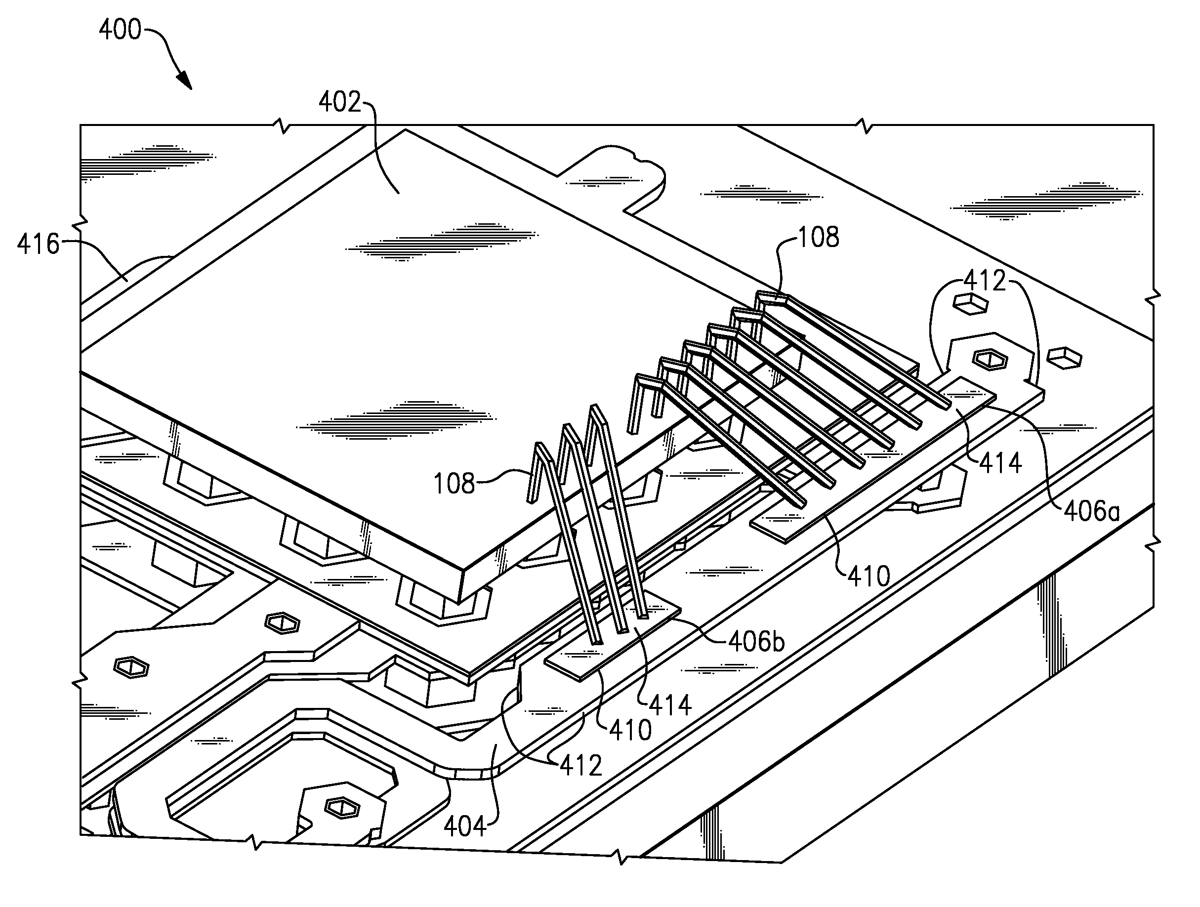
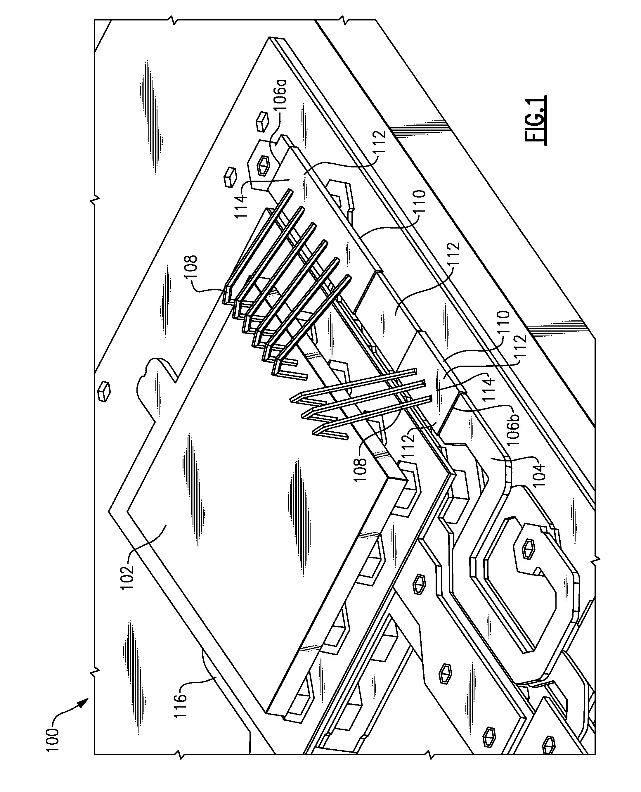
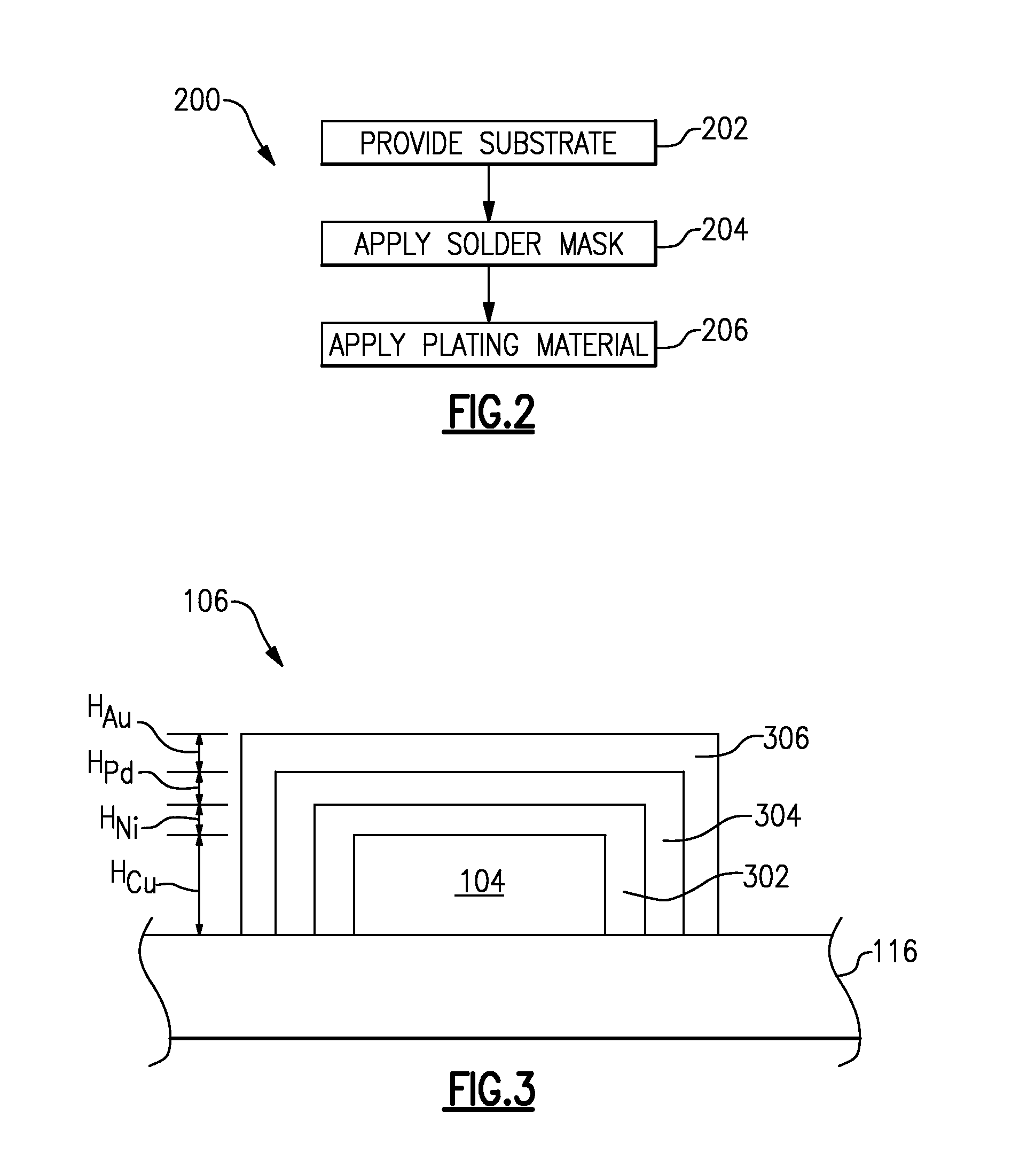
[0019]The features of the systems and methods will now be described with reference to the drawings summarized above. Throughout the drawings, reference numbers are re-used to indicate correspondence between referenced elements. The drawings, associated descriptions, and specific implementation are provided to illustrate embodiments of the inventions and not to limit the scope of the disclosure.

[0020]Wire bonding is a technique for connecting electrical circuit devices, for example, integrated circuit (IC) die, to the next level of packaging. These circuit devices generally comprise a plurality of small conductive leads / pads that are electrically connected, for example, by ball bonding, wedge bonding, or the like, to wire bond pads on conductors embedded in the device package or substrate. The wire bond pads on the substrate provide the electrical connections between the IC and the substrate, permitting the IC to interface with the outside world. In either type of wire bonding, the w...


PUM

PropertyMeasurementUnit
Lengthaaaaaaaaaa
Lengthaaaaaaaaaa
Lengthaaaaaaaaaa

Abstract

To reduce the RF losses associated with high RF loss plating, such as, for example, Ni/Pd/Au plating, the solder mask is reconfigured to prevent the edges and sidewalls of the wire-bond areas from being plated in some embodiments. Leaving the edges and sidewalls of the wire-bond areas free from high RF loss plating, such as Ni/Pd/Au plating, provides a path for the RF current to flow around the high resistivity material, which reduces the RF signal loss associated with the high resistivity plating material.

Description

BACKGROUND[0001]1. Field[0002]The present disclosure generally relates to the field of integrated circuit packaging, and more particularly to systems and methods of forming wire bond pads for packaging Radio Frequency (RF) integrated circuits (ICs).[0003]2. Description of the Related Art[0004]Silicon or other semiconductor wafers are fabricated into integrated circuits (ICs) as is known to one of ordinary skill in the art of IC fabrication. An IC is bonded and electrically connected to a carrier or substrate, which has layers of dielectric and metal traces, and packaged for use. A surface plating material is plated onto the top layer of copper traces to provide electrical connection points between the IC and the substrate, permitting the IC to interface with the outside world. Traditionally, nickel / gold (Ni / Au) has been a standard surface plating material for RFIC products and in certain situations, the RFIC is wire-bonded to the Ni / Au wire-bond pads plated on the surface of the sub...

Claims


Application Information

Patent Timeline
IPC IPC(8): H05K1/09H05K3/00C25D7/00C25D5/02C25D19/00
CPCC25D5/022H01L2224/05144C25D17/00H01L2924/014H05K1/0243H05K3/244H05K3/3452H05K2203/049H05K2203/0597H01L2924/01005H01L2224/45144C25D5/12H01L2224/03424H01L2924/01028H01L2924/01029H01L2924/14H01L2224/49111H01L2224/48095C25D7/0607H01L24/03H01L2924/1421H01L2224/05164H01L2224/05155H01L2224/05147H01L2924/2064H01L2224/04042H01L2224/03464H01L2224/03462H01L2924/00H01L24/49H01L24/85H01L2223/6605H01L2224/48644H01L2224/48655H01L2224/48664H01L2224/85205H01L2224/85411H01L2224/85416H01L2224/85444H01L2224/85447H01L2224/85455H01L2224/85464H01L2924/00011H01L2924/00014H01L2224/45147H01L24/45H01L2224/05644H01L24/48H01L2224/45015H01L2924/207H01L2224/45099H01L23/49838H01L23/49866H01L23/66H01L2223/6611H01L2224/48229H01L2924/01046H01L2924/01079H01L2924/15747H05K1/09H05K1/111H05K3/10
Inventor SUN, WEIMINZAMPARDI, PETER J.SHAO, HONGXIAO
Owner SKYWORKS SOLUTIONS INC
Why Eureka
Try Eureka