

Substrate treatment method
- Summary
- Abstract
- Description
- Claims
- Application Information
AI Technical Summary
Benefits of technology
Problems solved by technology
Method used
Image

Examples
first embodiment
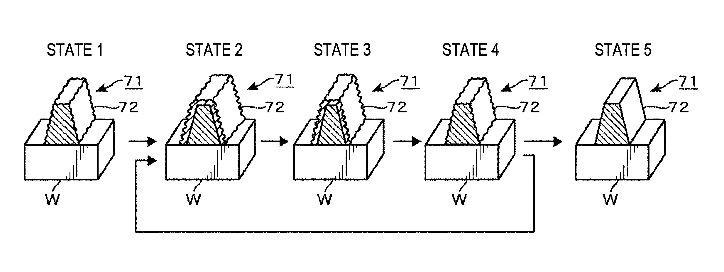
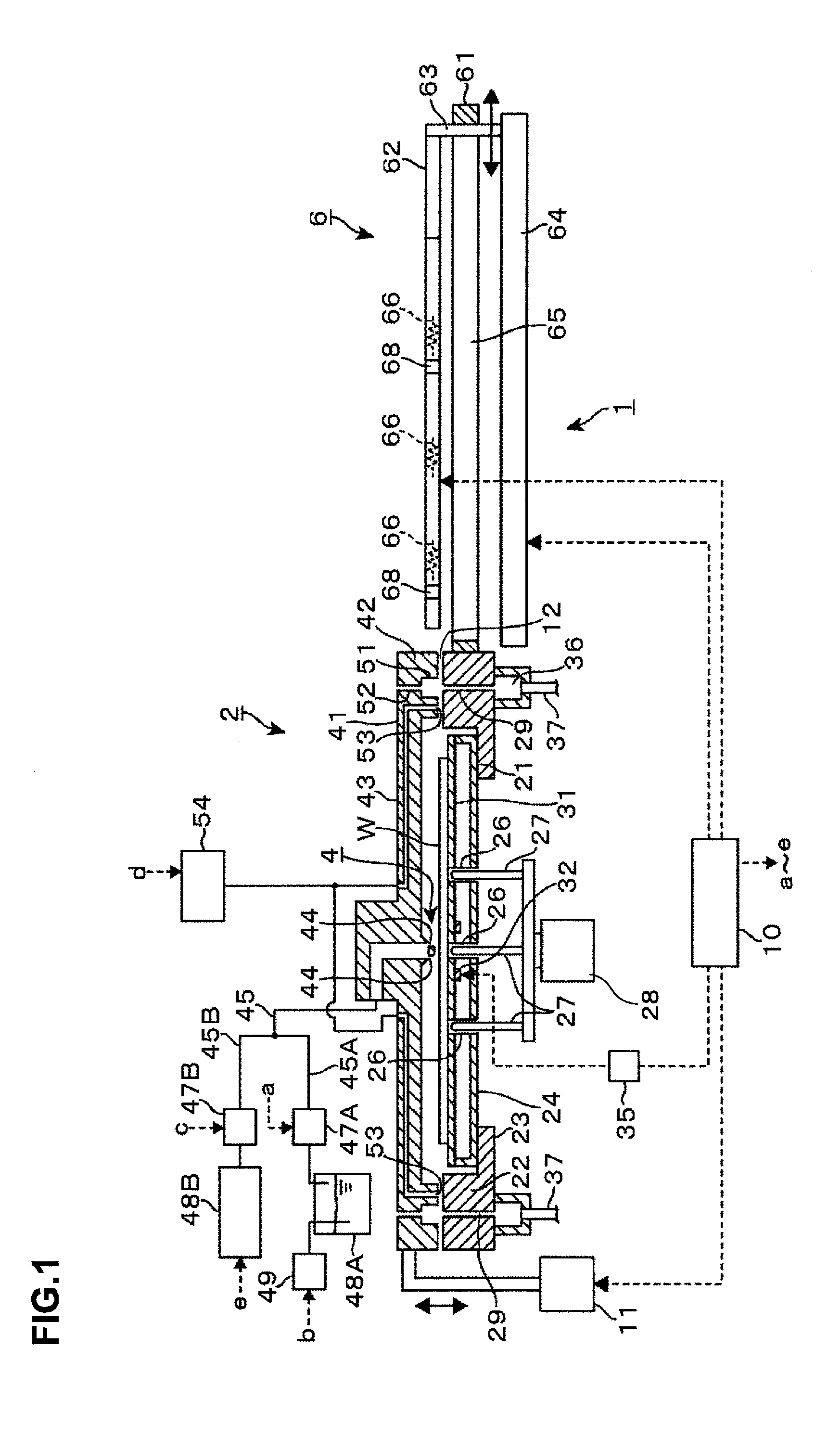
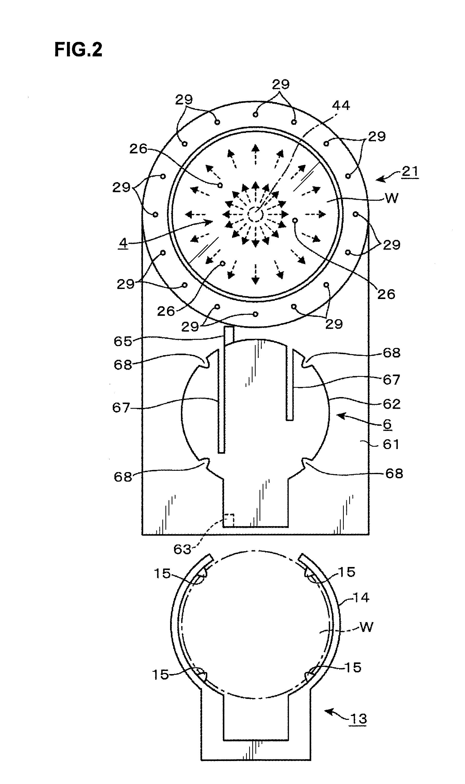
[0057]A solvent supply apparatus 1 according to an embodiment of the present invention will be described referring to FIG. 1 and FIG. 2 being a longitudinal side view and a transverse plan view thereof. The solvent supply apparatus 1 includes a treatment container 2 for treating a wafer W and a transfer mechanism 6 transferring the wafer W being a substrate between the treatment container 2 and the outside of the solvent supply apparatus 1. On the front surface of the wafer W transferred into the treatment container 2, a resist film has been formed. The resist film has undergone exposure and developing treatment and a resist pattern being a pattern mask has been formed in the resist film.
[0058]The treatment container 2 is formed in a flat circular shape and includes a container body 21 and a lid body 41. The container body 21 includes a side wall part 22 forming its peripheral edge portion and a bottom wall part 23 projecting inward from the lower end of the side wall part 22, and a...
modification examples
(Modification Examples of First Embodiment)
[0096]Hereinafter, modification examples of the first embodiment will be described. FIG. 19 illustrates a first modification example in which the heat source for heating the hot plate 31 is composed of an LED group 81. The LED group 81 is composed of many LEDs 82 provided below the whole hot plate 31, and each of the LEDs 82 irradiates the hot plate 31 with infrared light to thereby heat the hot plate 31. The LEDs 82 heating the center portion of the hot plate 31 surrounded by a dotted line 83 in the drawing in the LED group 81 are set higher in output than the other LEDs 82, whereby the center portion of the wafer W is heated to a temperature higher than that at the peripheral portion.
[0097]FIG. 20 illustrates a second modification example. The front surface of a hot plate 84 in FIG. 20 is curved such that the front surface at the center portion is higher in height than the front surface at the peripheral portion. Thus, the distance betwee...
second embodiment
[0102]Hereinafter, another embodiment will be described mainly for the different points from the first embodiment. In the solvent supply apparatus 1, the treatment container may be configured as illustrated in FIG. 24. FIG. 24 is a longitudinal side view of a treatment container 91 in which the treatment gas is supplied in a direction different from that in the treatment container 2. A lid body 92 constituting the treatment container 91 is provided with a ring-shaped gas discharge port 93 outside the wafer W in a manner to surround the wafer W. Further, an exhaust port 94 is opened above the center portion of the wafer W so that the treatment gas and the drying gas discharged from the gas discharge port 93 flow to the center portion of the wafer W and are exhausted from the exhaust port 94 as indicated with arrows in the drawing. A numeral 95 in the drawing denotes a sealing material.
[0103]The treatment gas discharged from the gas discharge port 93 gathers to the center portion of t...
PUM
| Property | Measurement | Unit |
|---|---|---|
| Temperature | aaaaa | aaaaa |
| Height | aaaaa | aaaaa |
| Surface roughness | aaaaa | aaaaa |
Abstract
Description
Claims
Application Information