Substrate carrier with multiple emissivity coefficients for thin film processing

a carrier and emissivity coefficient technology, applied in the direction of polycrystalline material growth, crystal growth process, manufacturing tools, etc., can solve the problem of difficult epitaxial growth of such structures, and achieve the effect of high emissivity treatment, enhanced heat source transfer, and high emissivity material

Inactive Publication Date: 2012-09-13
APPLIED MATERIALS INC
View PDF0 Cites 9 Cited by
  • Summary
  • Abstract
  • Description
  • Claims
  • Application Information

AI Technical Summary

Benefits of technology

[0018]Substrate carrier for support of a substrate during a deposition process and having multiple emissivity coefficients is described. A front side of the carrier has a first carrier surface upon which the substrate is to be disposed. The first carrier surface has at least a first emissivity coefficient different than a second emissivity coefficient of a second carrier surface on the front side of the carrier and adjacent to the first carrier surface. Selection of the ...

Problems solved by technology

While LEDs employing multiple quantum well (MQW) structures epitaxially grown on a substrate are a promising technology, epitaxial growth of such struc...

Method used


Image

  • Substrate carrier with multiple emissivity coefficients for thin film processing
  • Substrate carrier with multiple emissivity coefficients for thin film processing
  • Substrate carrier with multiple emissivity coefficients for thin film processing

Examples


Embodiment Construction

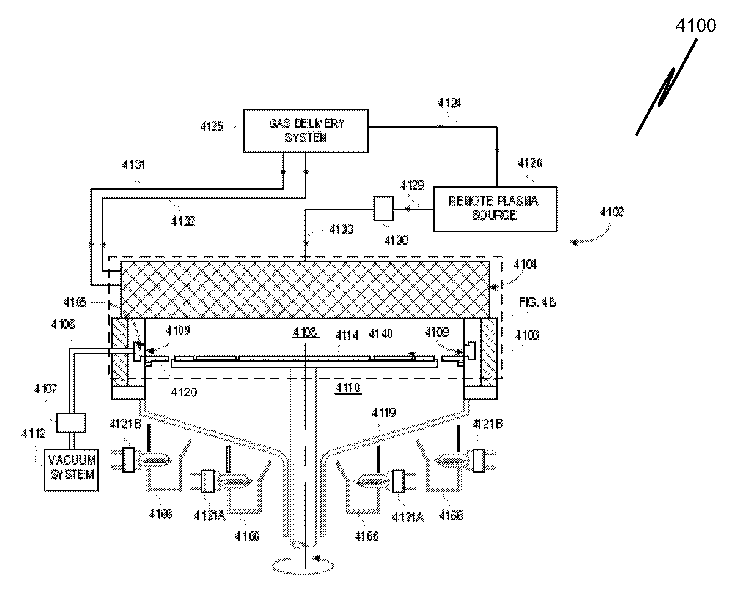
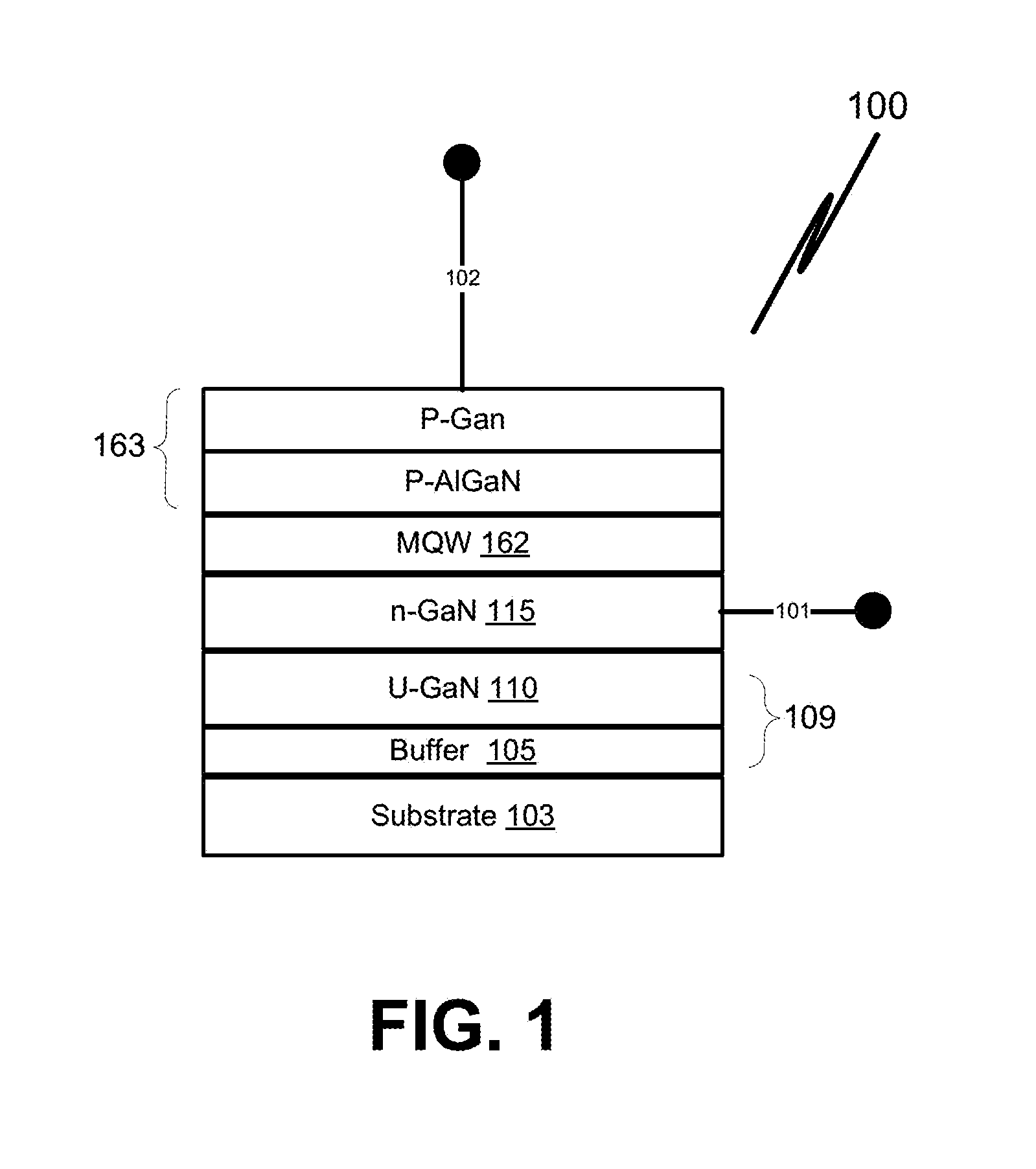
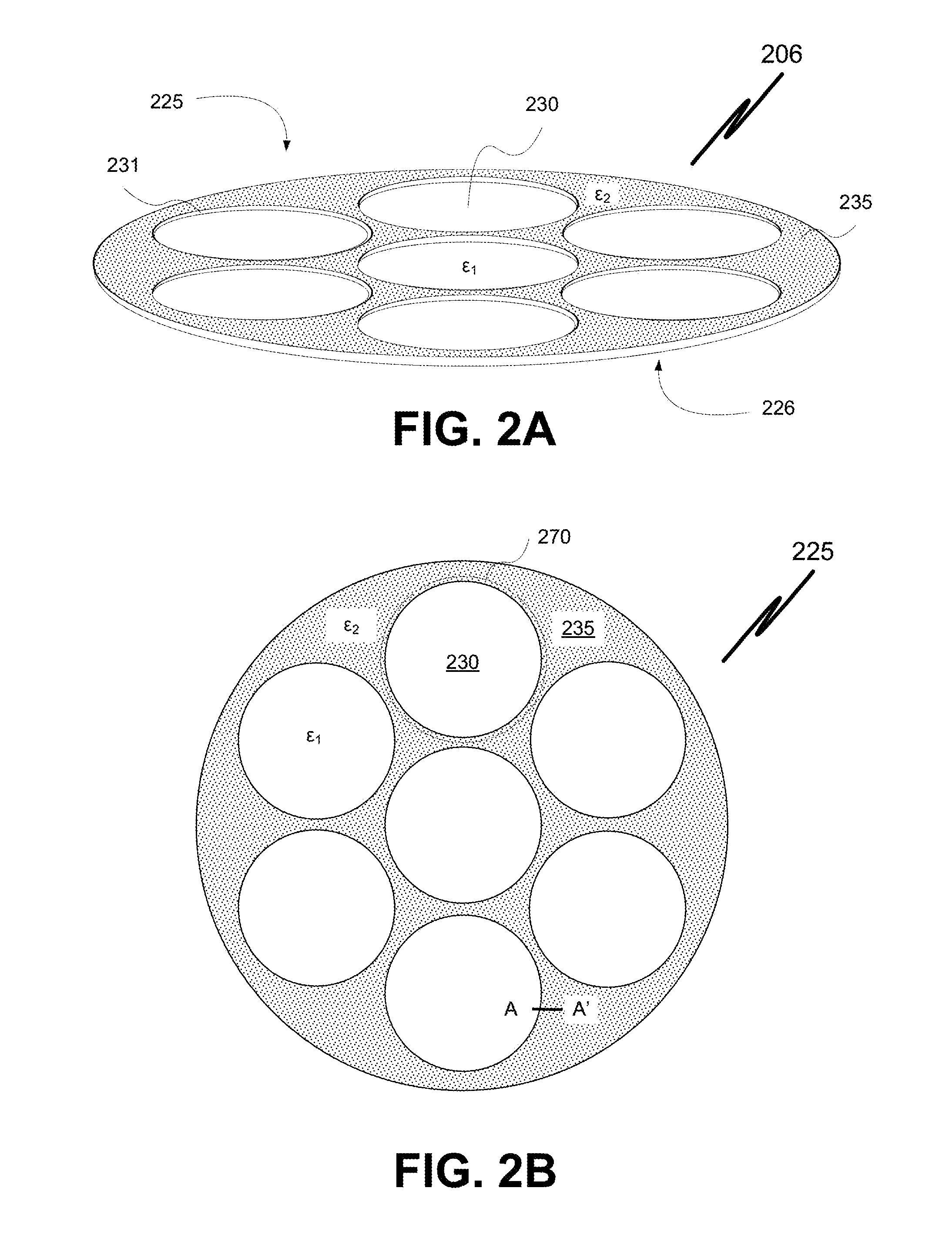
[0021]In the following description, numerous details are set forth. It will be apparent, however, to one skilled in the art, that the present invention may be practiced without these specific details. In some instances, well-known methods and devices are shown in block diagram form, rather than in detail, to avoid obscuring the present invention. Reference throughout this specification to “an embodiment” means that a particular feature, structure, function, or characteristic described in connection with the embodiment is included in at least one embodiment of the invention. Thus, the appearances of the phrase “in an embodiment” in various places throughout this specification are not necessarily referring to the same embodiment of the invention. Furthermore, the particular features, structures, functions, or characteristics may be combined in any suitable manner in one or more embodiments. For example, a first embodiment may be combined with a second embodiment anywhere the two embod...


PUM

PropertyMeasurementUnit
Temperatureaaaaaaaaaa
Distanceaaaaaaaaaa
Surface areaaaaaaaaaaa

Abstract

Substrate carrier having multiple emissivity coefficients for thin film processing and more particularly for support of a substrate during a deposition process epitaxially growing a film on the substrate. A front side of the carrier has a first carrier surface upon which the substrate is to be disposed, the first carrier surface having a first emissivity coefficient different than a second emissivity coefficient of a second carrier surface adjacent to the first carrier surface. Selection of the second emissivity coefficient independent of the first emissivity coefficient may modify an amount of energy radiated from the second carrier surface during processing of the substrate. In one embodiment, the second carrier surface has a second emissivity coefficient which is lower than the first emissivity coefficient to reduce heat loss from the carrier surface while maintaining high efficiency energy transfer between the carrier and a substrate.

Description

CROSS REFERENCE TO RELATED APPLICATIONS[0001]This application claims the benefit of U.S. Provisional Application No. 61 / 451,534 (Attorney Docket No. 015625L / NEON / ESONG) filed on Mar. 10, 2011, entitled “SUBSTRATE CARRIER WITH MULTIPLE EMISSIVITY COEFFICIENTS FOR THIN FILM PROCESSING,” the entire contents of which are hereby incorporated by reference in its entirety for all purposes.BACKGROUND[0002]1. Field[0003]Embodiments of the present invention pertain to the field of thin film epitaxial growth, and more particularly to carriers for supporting substrates during epitaxial growth of thin films.[0004]2. Description of Related Art[0005]Group III-V materials are playing an ever increasing role in the semiconductor and related, e.g. light-emitting diode (LED), industries. While LEDs employing multiple quantum well (MQW) structures epitaxially grown on a substrate are a promising technology, epitaxial growth of such structures is difficult because epitaxial growths are often very sensit...

Claims


Application Information

Patent Timeline
IPC IPC(8): C30B25/12B05D5/00B24B1/00C30B25/02
CPCC30B25/12C30B29/403H01L21/68771H01L21/67115H01L21/68764H01L21/67103
Inventor HUANG, JUNO YU-TINGSHRAUTI, SURESH M.DUBOUST, ALAINBOUR, DAVIDHSU, WEI-YUNGCHEN, LIANG-YUN
Owner APPLIED MATERIALS INC
Why Eureka
Try Eureka