
Method for producing a nanostructured funcitonal coating and a coating that can be produced according to said method

a technology of nanostructured funcitonal coatings and nanostructured layers, which is applied in the direction of manufacturing tools, other chemical processes, natural mineral layered products, etc., can solve the problems of reducing the adhesion strength, and reducing the wear resistance of these coatings by increasing the hardness,

Inactive Publication Date: 2005-01-20
ROBERT BOSCH GMBH +1
View PDF25 Cites 58 Cited by
  • Summary
  • Abstract
  • Description
  • Claims
  • Application Information

AI Technical Summary

Benefits of technology

[0010] The method according to the present invention for producing a nanostructured functional coating has the advantage over the related art that, because of the pulsed plasma source used, a substantially higher ion density is achieved in the plasma; i.e., it is now possible in a simple way to produce coatings that require a high ion density during deposition. The deposition of such coatings is only possible in conventional PACVD processes with the help of an additional ionization source, which may now be omitted.
[0012] Another advantage of the method according to the present invention is that because of the pulsed plasma source employed and the resulting higher ionization of the materials or atoms utilized for coating, the surface energy in the vicinity of the substrate to be coated is adjustable in a controlled manner to a level necessary for forming the desired nanostructured texture.
[0013] In addition, the method according to the present invention has the advantage of a generally simpler process technology, using a reduced number of system components. For example, it now permits a largely charge-independent and component-independent process management; that is, it is significantly more flexible than known RF techniques, i.e., methods that work with a high frequency substrate electrode voltage.
[0014] Finally, another significant advantage of the method according to the present invention is that the substrate and / or the functional coating deposited on it are heated during production of the coating only to temperatures of a maximum of 250° C., in particular less than 200° C. In this respect it is often possible to dispense entirely with additional cooling of the substrate during deposition of the coating, or only a conventional cooling device having a comparatively low cooling capacity is needed.
[0015] The nanostructured functional coating according to the present invention has the advantage that, in contrast to the coatings known from the related art, which are produced for example by CVD methods, it is producible free of unwanted reaction residues such as residues of chlorine or sulfur from corresponding process gases. In particular, in the functional coatings produced in particular by the method according to the present invention, besides the elements that define the composition of the functional coating produced; such as O, H, N, C and / or other metals, only the noble gas utilized as plasma gas is detectable.

Problems solved by technology

Disadvantages of such coatings are the often relatively high coefficients of friction, occurrence of intrinsic tensions and resulting reduction of adhesive strength, and the great brittleness in comparison to the hardness.
Furthermore, improving the wear-resistance of these coatings by increasing the hardness has a detrimental effect on other desired properties, such as toughness, impact resistance and substrate adhesion.
However, their disadvantages include their relatively low abrasion resistance, inadequate resistance to media, and limited temperature resistance, less than 350° C. in the case of DLC.

Method used


Image

  • Method for producing a nanostructured funcitonal coating and a coating that can be produced according to said method
  • Method for producing a nanostructured funcitonal coating and a coating that can be produced according to said method

Examples


Embodiment Construction

[0023] The present invention is based on a coating system 5 represented in FIG. 1, as described in similar form in M. Diserens et al., Interface and Coatings Technology,

[0024]108 to 109 (1998), p. 242.

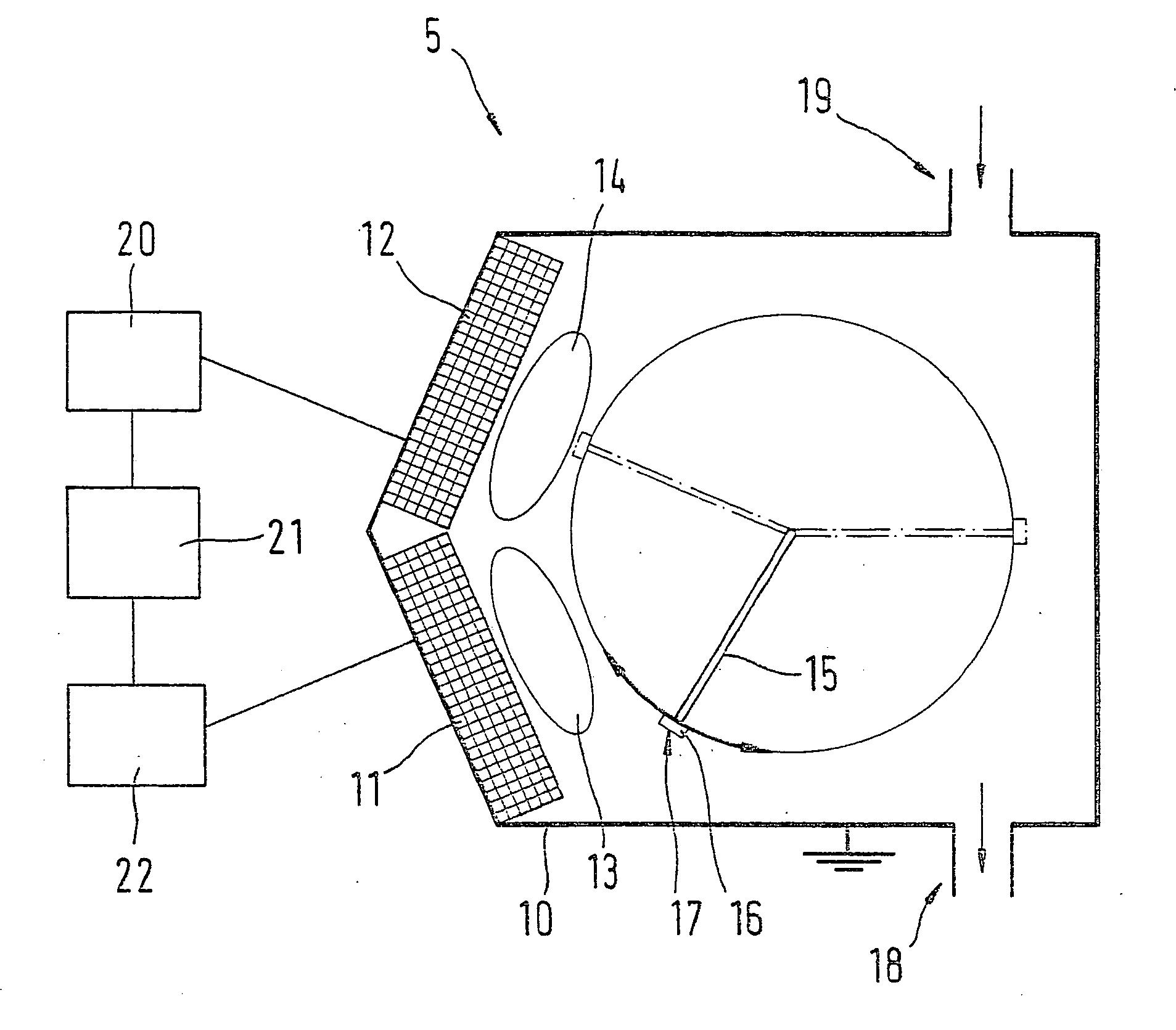
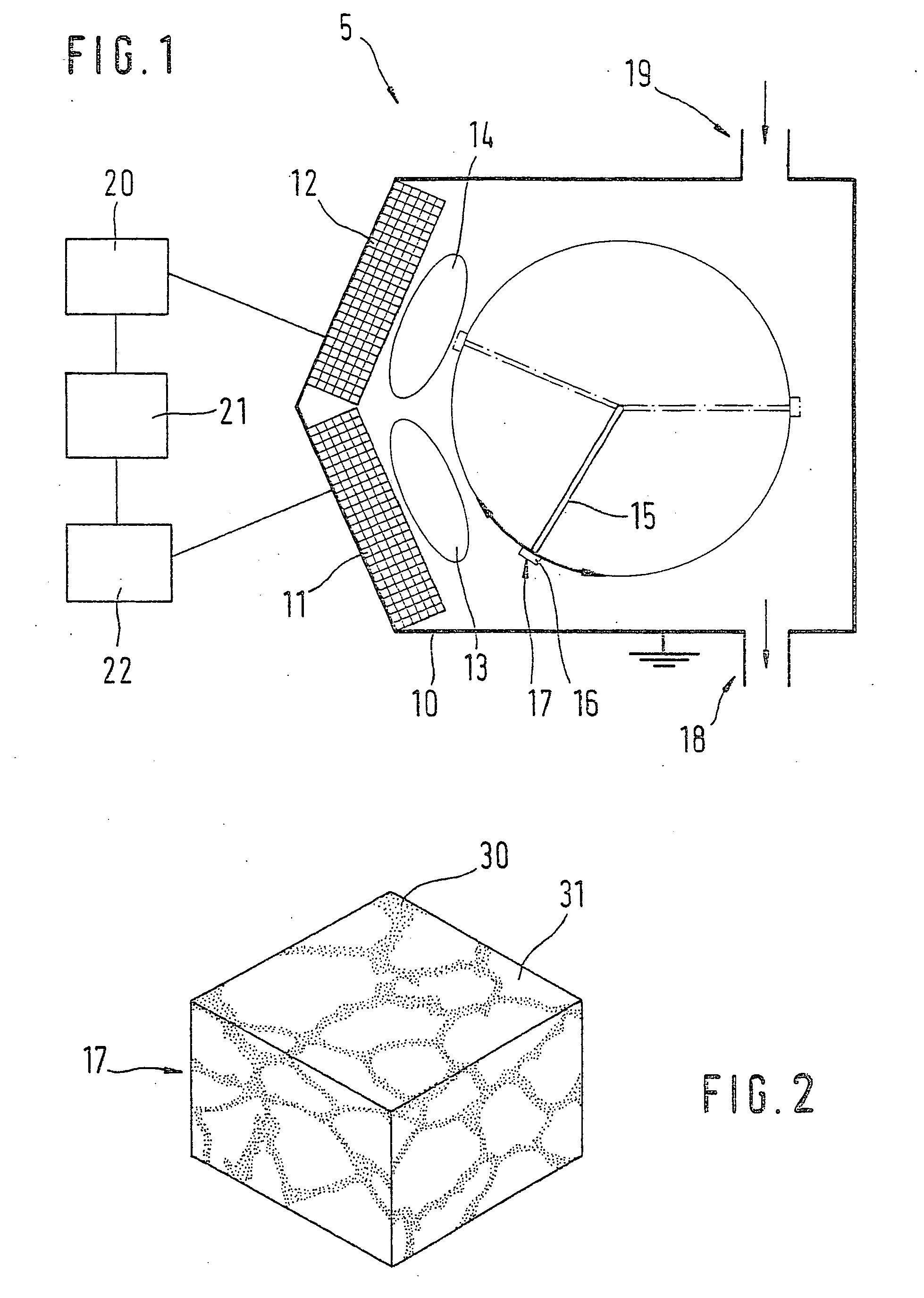
[0025] In detail, coating system 5 has a grounded vacuum chamber 10, a first plasma source 11, a second plasma source 12, a substrate support 15 with a substrate 16 on it, a gas outlet 18 and a gas inlet 19. The design also provides for first plasma source 11 to be used in producing a first plasma 13 that is associated with it, and for second plasma source 12 to be used in producing a second plasma 14 that is associated with it, from which plasmas a coating 17 is deposited on the surface of substrate 16 via a material-input.

[0026]FIG. 1 also shows that first plasma source 11 is connected to a first high voltage source 22 and second plasma source 12 to a second high voltage source 20, with whose aid plasma sources 11, 12 are each pulsable initially independently of each other. In add...


PUM

PropertyMeasurementUnit
frequencyaaaaaaaaaa
frequencyaaaaaaaaaa
frequencyaaaaaaaaaa

Abstract

A method for producing a nanostructured, in particular a ceramic-like functional coating on a substrate is described. To that end, using at least one plasma source, a pulsed plasma is produced with which a matrix phase and at least one nano-scale interstitial phase embedded in it are deposited on the substrate via a material input. Preferably a plurality of pulsed plasma sources that are time-correlated or synchronized with each other are used. Also proposed is a nanostructured functional coating, in particular one producible by this method, which is free of chlorine and / or sulfur, and which contains at least one metal and / or at least one element selected from the group oxygen, hydrogen, nitrogen, carbon, helium, argon or neon.

Description

FIELD OF THE INVENTION [0001] The present invention relates to a method for producing a nanostructured, in particular a ceramic-like functional coating on a substrate, and a nanostructured functional coating producible using the method. BACKGROUND INFORMATION [0002] Wear-protection coatings, in particular in the form of coatings of hard material based on a carbonitride, are known in single-layer or multiple-layer structure with layer thicknesses in the micron range, both on tools and on parts. [0003] Disadvantages of such coatings are the often relatively high coefficients of friction, occurrence of intrinsic tensions and resulting reduction of adhesive strength, and the great brittleness in comparison to the hardness. Furthermore, improving the wear-resistance of these coatings by increasing the hardness has a detrimental effect on other desired properties, such as toughness, impact resistance and substrate adhesion. [0004] In addition to hard material coatings based on a carbonitr...

Claims


Application Information

Patent Timeline
Patent Type & Authority Applications(United States)
IPC IPC(8): B23B51/00B23B27/14B23P15/28C23C14/06C23C14/34C23C14/35
CPCC23C14/06C23C14/352Y10T428/30Y10T428/252Y10T428/25C23C14/354
Inventor BECK, THOMASSCHATTKE, ALEXANDERHENKE, SASCHASCHIER, VEIT
Owner ROBERT BOSCH GMBH
Learn More