Method and apparatus for the selective deposition of epitaxial germanium stressor alloys

a stressor alloy and selective deposition technology, applied in the direction of crystal growth process, polycrystalline material growth, chemically reactive gas growth, etc., can solve the problem of less resistivity, less electronic properties of the channel, and increased threshold voltage, so as to reduce the adhesion of exhaust components

Active Publication Date: 2012-10-04
APPLIED MATERIALS INC
View PDF5 Cites 204 Cited by
  • Summary
  • Abstract
  • Description
  • Claims
  • Application Information

AI Technical Summary

Benefits of technology

[0006]Method and apparatus for forming stressor layers on a semiconductor substrate are provided. A germanium stressor layer may be formed on a substrate by positioning the substrate in a processing chamber, flowing a germanium precursor into the processing chamber, forming a stressor precursor outside the processing chamber, flowing the stressor precursor into the processing chamber, and growing the germanium stressor layer epitaxially on the substrate. An apparatus for forming such layers includes a rotating substrate support disposed in an enclosure, a plurality of gas inlets formed in a wall of the enclosure, a least one gas outlet formed in a wall of the enclosure, a reactive or non-reactive source for generating a stressor precursor coupled to a gas inlet by a first conduit, a non-reactive source for providing a germanium precursor coupled to a gas inlet by a second conduit, and a heated exhaust system. The heated exhaust system may have a coating applied to reduce adhesion of exhaust components, and may include a condensation trap.
[0007]The germanium precursor may be a hydride, and the stressor precursor may be a metal halide. A selectivity control species, for example a halide gas, may be included with the reaction mixture to control deposition selectivity on semiconductive and dielectric regions of the substrate.

Problems solved by technology

As device geometries decline according to Moore's Law, the size of transistor components poses challenges to engineers working to make devices that are smaller, faster, use less power, and generate less heat.
For example, as the size of a transistor declines, the channel region of the transistor becomes smaller, and the electronic properties of the channel become less viable, with more resistivity and higher threshold voltages.

Method used


Image

  • Method and apparatus for the selective deposition of epitaxial germanium stressor alloys
  • Method and apparatus for the selective deposition of epitaxial germanium stressor alloys
  • Method and apparatus for the selective deposition of epitaxial germanium stressor alloys

Examples


Embodiment Construction

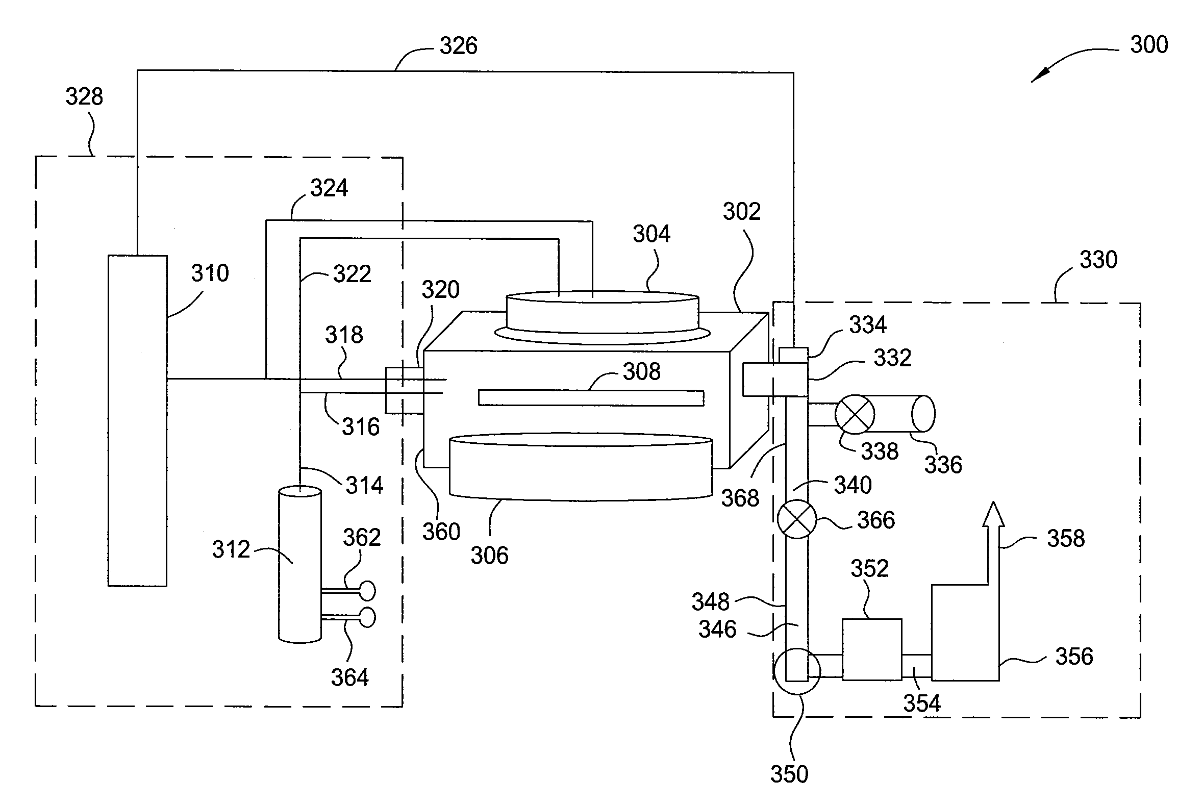
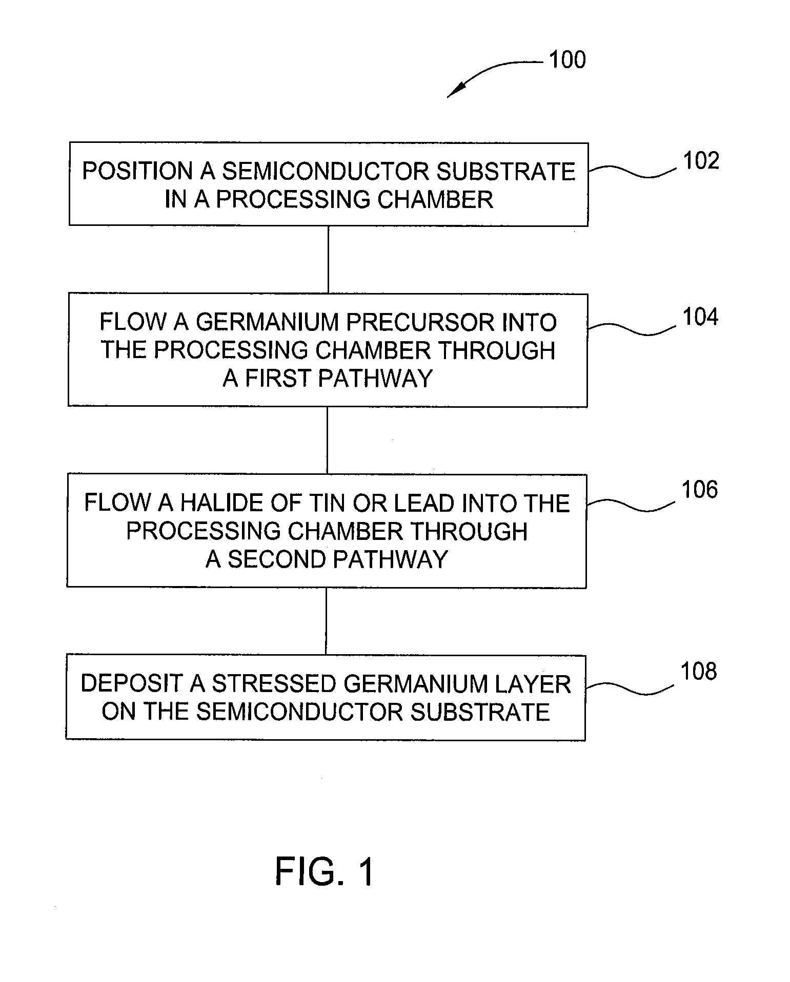
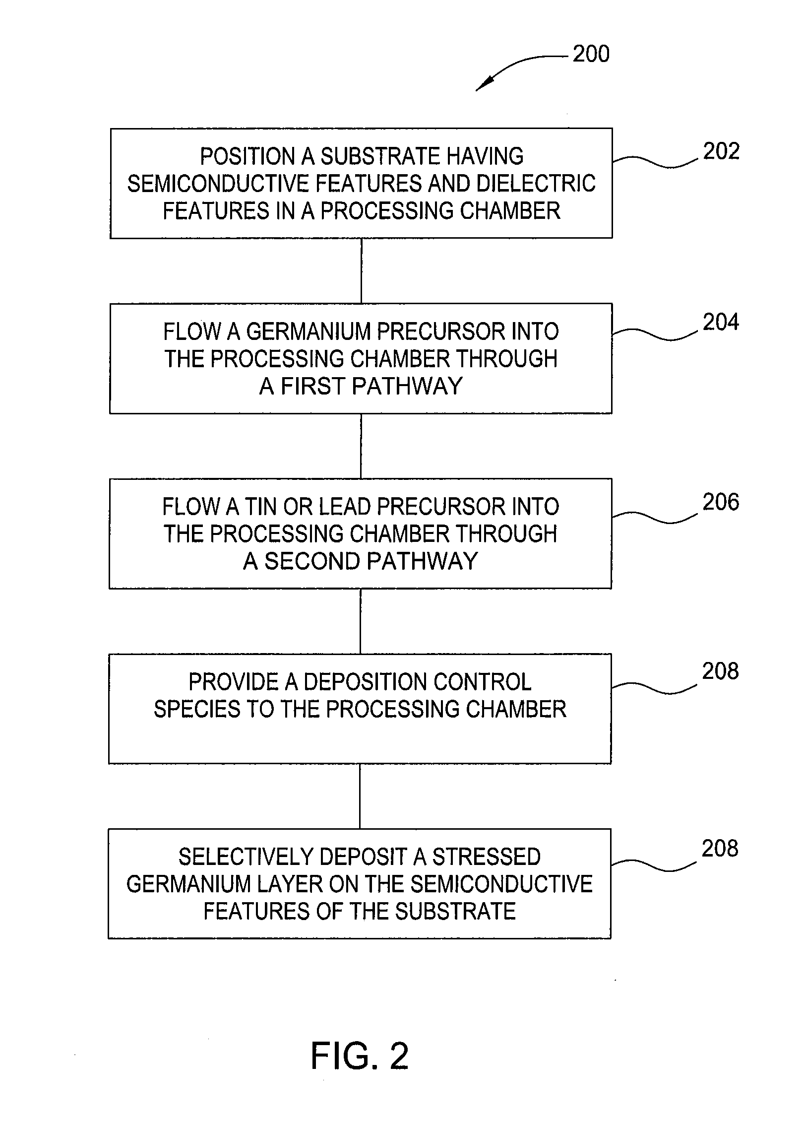
[0013]FIG. 1 is a flow diagram summarizing a method 100 according to one embodiment. A semiconductor substrate is positioned in a processing chamber at 102. The semiconductor substrate may be any semiconductive material on which a stressor layer is to be formed. A silicon substrate on which a transistor structure is to be formed may be used in one example. The semiconductor substrate may have dielectric areas formed on a surface thereof in some embodiments. For example, a silicon substrate may have transistor gate structures and dielectric spacers formed adjacent to semiconductive source / drain regions, which may be regions of doped silicon or regions on which source / drain materials are to be formed. Thus, the source / drain regions may comprise the stressor layers described herein in addition to, or instead of, doped silicon layers.

[0014]The stressor layers described herein typically comprise metal atoms disposed in a germanium matrix, GexMy. Large metal atoms, for example group IV me...


PUM

PropertyMeasurementUnit
temperatureaaaaaaaaaa
pressureaaaaaaaaaa

Abstract

A method and apparatus for forming heterojunction stressor layers is described. A germanium precursor and a metal precursor are provided to a chamber, and an epitaxial layer of germanium-metal alloy formed on the substrate. The metal precursor is typically a metal halide, which may be provided by subliming a solid metal halide or by contacting a pure metal with a halogen gas. The precursors may be provided through a showerhead or through a side entry point, and an exhaust system coupled to the chamber may be separately heated to manage condensation of exhaust components.

Description

CROSS-REFERENCE TO RELATED APPLICATIONS[0001]This application claims benefit of U.S. Provisional Patent Application Ser. No. 61 / 468,443 filed Mar. 28, 2011, which is herein incorporated by reference.BACKGROUND OF THE INVENTION[0002]1. Field of the Invention[0003]Technology described herein relates to manufacture of semiconductor devices. More specifically, methods are described of forming field effect transistors using strained materials.[0004]2. Description of the Related Art[0005]Germanium was one of the first materials used for semiconductor applications such as CMOS transistors. Due to vast abundance of silicon compared to germanium, however, silicon has been the overwhelming semiconductor material of choice for CMOS manufacture. As device geometries decline according to Moore's Law, the size of transistor components poses challenges to engineers working to make devices that are smaller, faster, use less power, and generate less heat. For example, as the size of a transistor dec...

Claims


Application Information

Patent Timeline
Patent Type & Authority Applications(United States)
IPC IPC(8): C30B25/02C30B25/10C30B25/16C30B25/12C30B25/08C30B25/14
CPCC30B25/14C30B29/52C30B25/16H01L21/20H01L21/205H01L21/8238C23C16/08C23C16/4412C23C16/4584C23C16/4586C30B23/02C30B23/06C30B23/063C30B23/066C30B25/10C30B29/08H01L21/02381H01L21/02532H01L21/02581H01L21/02636H01L29/1054
Inventor SANCHEZ, ERROL ANTONIO C.CARLSON, DAVID K.
Owner APPLIED MATERIALS INC
Why Eureka
Try Eureka