photodetector

a photodetector and photoelectric technology, applied in the field of photodetectors, can solve the problems of large error in multiplication factor, difficult to precisely control the temperature dependence of apd, and cannot cope with changes in other environmental factors

Inactive Publication Date: 2012-10-04
TOYOTA JIDOSHA KK
View PDF3 Cites 8 Cited by
  • Summary
  • Abstract
  • Description
  • Claims
  • Application Information

AI Technical Summary

Benefits of technology

[0021]According to the present invention, the photodetector utilizing the avalanche effect can appropriately perform the temperature compensation of the multiplication factor.

Problems solved by technology

Therefore, it becomes a problem in an application field where a wide operating temperature range is required.
Furthermore, when the applied voltage is enhanced for retaining a high current amplification factor, a slight change in the applied voltage causes a large error in the multiplication factor.
However, in the above technologies, a secondary section of the temperature dependency is not considered, which makes it difficult to precisely control the temperature dependency of the APD.
Moreover, they cannot cope with changes in other environmental factors such as moisture and aging.
Furthermore, in the above technologies, a relationship between the voltage slightly smaller than the breakdown voltage and the avalanche multiplication factor is not clear, and therefore the accuracy of the control is poor.
Still furthermore, in the above technologies, when the reference light source is used, a highly precise calibration of the light source is required, and noise emitted from the reference light source exerts a harmful influence on S / N ratio in the signal detection.
Moreover, the technologies of using the reference light receiving element can scarcely be utilized when a weak and high-speed optical signal can only be obtained.

Method used


Image

  • photodetector
  • photodetector
  • photodetector

Examples


first embodiment

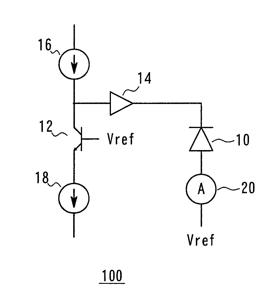
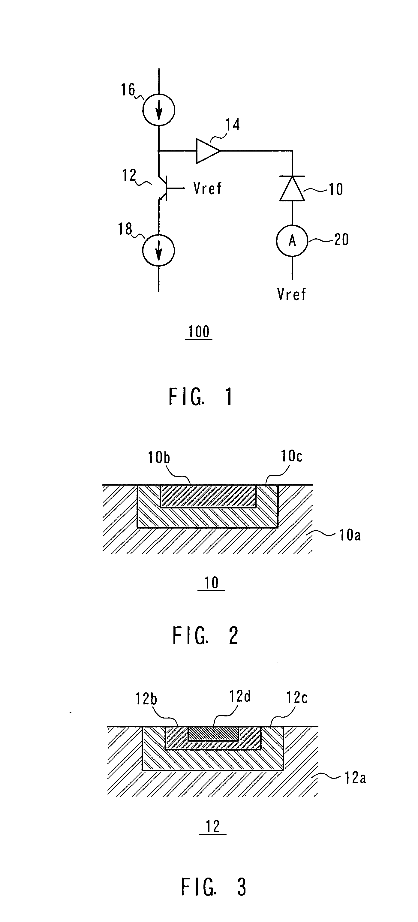
[0032]A photodetector 100 comprises, as shown in FIG. 1, an avalanche photodiode (APD) 10, an avalanche transistor (AT) 12, a buffer element 14, a first current source 16, a second current source 18 and an ammeter 20.

[0033]The APD 10 comprises, as shown in a cross-sectional view of elements in FIG. 2, a semiconductor substrate 10a, a first well 10b, and a second well 10c. As the semiconductor substrate 10a, there can be utilized a silicon substrate, a gallium arsenide substrate or the like. The second well 10c is formed by adding a dopant of a conductivity type opposite to that of the semiconductor substrate 10a, to the surface area of the semiconductor substrate 10a. The first well 10b is formed by adding a dopant of a conductivity type opposite to that of the second well 10c, into the forming area of the second well 10c formed on the surface area of the semiconductor substrate 10a, more shallowly than in the case of the second well 10c. Consequently, the first well 10b and the se...

second embodiment

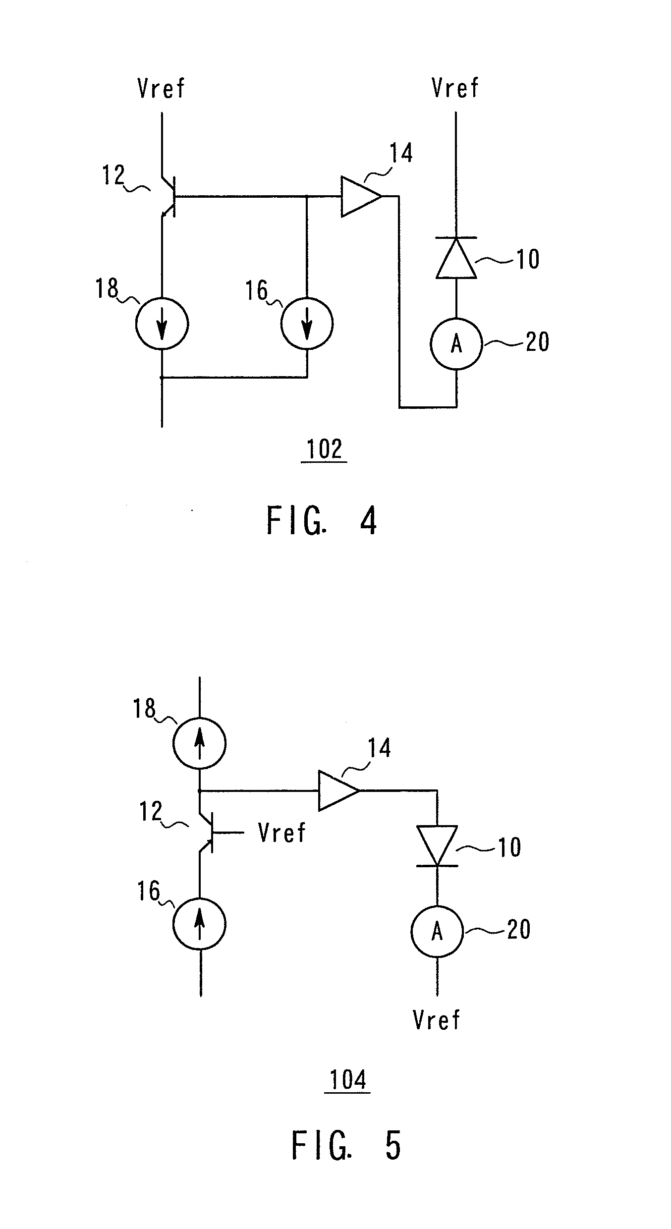
[0072]On the other hand, in an identical manner to the photodetector 200 in the constitution of the second embodiment, the photodetection is performed by applying light to the collector-base junction of the AT 12. Here, if a signal light frequency is sufficiently higher than an AC reference current frequency, a photoelectric current can be separated from a current based on the AC reference current Iac, followed by detection.

[0073]Also in the constitution of the present embodiment, connection to the collector of the AT 12 may be performed. Further, also in the constitution of the present embodiment, the reference current and the signal current are separated from each other by a frequency division system, but the separation may be performed by a time-sharing system. Furthermore, the AT 12 may be a transistor having a structure as shown in FIG. 8. In addition, in the constitution of the present embodiment the AT 12 is an NPN transistor, but it may be a PNP transistor as in the case of ...


PUM


Abstract

A photodetector disclosed herein comprises an avalanche transistor having a reference junction structure in which temperature characteristics of a current amplification factor are about the same as those of an avalanche photodiode and which is reverse-biased, and a current injection junction structure which injects a reference current to the reference junction structure and which is forward-biased. Voltages to be applied to the avalanche photodiode and the reference junction structure are controlled so that the amplification factor of the reference current amplified in the reference junction structure is retained at a predetermined value, whereby the temperature characteristics of the photodetector utilizing an avalanche effect can be stabilized.

Description

TECHNICAL FIELD[0001]The present invention relates to a photodetector, and more particularly, it relates to a photodetector utilizing an avalanche effect.BACKGROUND ART[0002]An avalanche photodiode (APD) is used as a light receiving element for detecting a weak optical signal in optical communications, optical radar and the like. When photons enter the APD, electron-hole pairs are generated, and the electrons and positive holes are accelerated by a high electric field, so that collision and ionization successively occur one after another like an avalanche, thereby generating new electrode-hole pairs.[0003]As use modes of the APD, there are a linear mode where the APD is operated at a reverse bias voltage less than a breakdown voltage, and a Geiger mode where the APD is operated at the breakdown voltage or more. In the linear mode, a rate of the annihilated electron-hole pairs (going out from the high electric field) is larger than a rate of the generated electron-hole pairs, so that...

Claims


Application Information

Patent Timeline
Patent Type & Authority Applications(United States)
IPC IPC(8): H01L31/107
CPCH03F3/08H01L31/02027
Inventor ITO, KOTASOGA, MINEKINICLASS, CRISTIANOPOPOVIC, RADIVOJE S.LANY, MARCKINDO, TOSHIKI
Owner TOYOTA JIDOSHA KK
Why Eureka
Try Eureka