Vertically structured group iii nitride semiconductor LED chip and method for manufacturing the same

a semiconductor led chip and nitride technology, applied in semiconductor/solid-state device manufacturing, semiconductor devices, electrical equipment, etc., can solve the problems of high nitrogen dissociation pressure, high output, and difficulty in bulk single crystal growth, so as to reduce the stress applied to each light-emitting structure, reduce the incidence of cracks, and high quality

Active Publication Date: 2012-10-04
DOWA ELECTRONICS MATERIALS CO LTD
View PDF1 Cites 13 Cited by
  • Summary
  • Abstract
  • Description
  • Claims
  • Application Information

AI Technical Summary

Benefits of technology

[0040]In the present invention, a light emitting structure is formed to have a top view shape of a circle or a 4n-gon having rounded corners (n is a positive integer. In other words, 4n means a multiple of 4), to distribute the stress applied to the light emitting structure. Further, a plurality of through grooves or through holes are formed in a conductive support to perform pseudo isolation between the boundaries on the conductive support, which define each light emitting structure. Thus, the stress applied to the light emitting structure from the conductive support side is distributed and the stress applied to each light emitting structure is reduced, which prevents the light emitting structure supported by the conductive support from being cracked when detached from a sapphire substrate at the time of the lift-off. Consequently, incidence of cracks is reduced and high quality vertical LED chips without cracks in the light emitting structure can be provided at a high yield.
[0041]In the present invention, a primary isolation of a light emitting laminate made of a Group III nitride semiconductor on the sapphire substrate is performed in accordance with the size of the LED chips to be formed. Since the conductive support still remains as a wafer even after a growth substrate is removed by lift-off, device processing can be performed in post-processes.

Problems solved by technology

On the other hand, a Group III nitride semiconductor using Al, Ga, In, etc. as a Group III element and using N as a Group V element has a high melting point and high nitrogen dissociation pressure, which makes it difficult to perform bulk single crystal growth.
Further, since there are no inexpensive large diameter conductive single crystal substrates available, such a semiconductor is typically formed on a sapphire substrate.
Further, since the sapphire substrate has low thermal conductivity, heat generated in the light emitting structure is not sufficiently dissipated, which (4) causes a heat saturation problem in LED characteristics, and is disadvantageous in achieving high output.
However, the technique disclosed in Patent Document 1 is considered to limit the effect of extracting light through a side surface to the case of small chip size.
This specifically applies only to chips having a small size such as 350 μm or less, and however contradicts in case of the higher output due to increased chip size.
If the sapphire substrate is removed with the support portions and the light emitting structures being separated, chips would fall apart; accordingly, subsequent processes such as the manufacturing of an n-type electrode would be complicated and the yield would be reduced.
So, the dimensional accuracy and ensuring the shape of a metal support layer formed by plating are difficult.
And, etching of the light emitting structure using the metal support layer formed by plating as a mask makes it difficult to achieve dimensional accuracy and ensuring the shape.
Furthermore, since the reflective ohmic metal (ohmic contact layer) is also etched using the mask, metal residue would attach to a side surface of the light emitting laminate; thus, LED chip characteristics would be adversely affected by a short circuit, leakage current, or the like.

Method used


Image

  • Vertically structured group iii nitride semiconductor LED chip and method for manufacturing the same
  • Vertically structured group iii nitride semiconductor LED chip and method for manufacturing the same
  • Vertically structured group iii nitride semiconductor LED chip and method for manufacturing the same

Examples


example

Experimental Examples 1 to 8

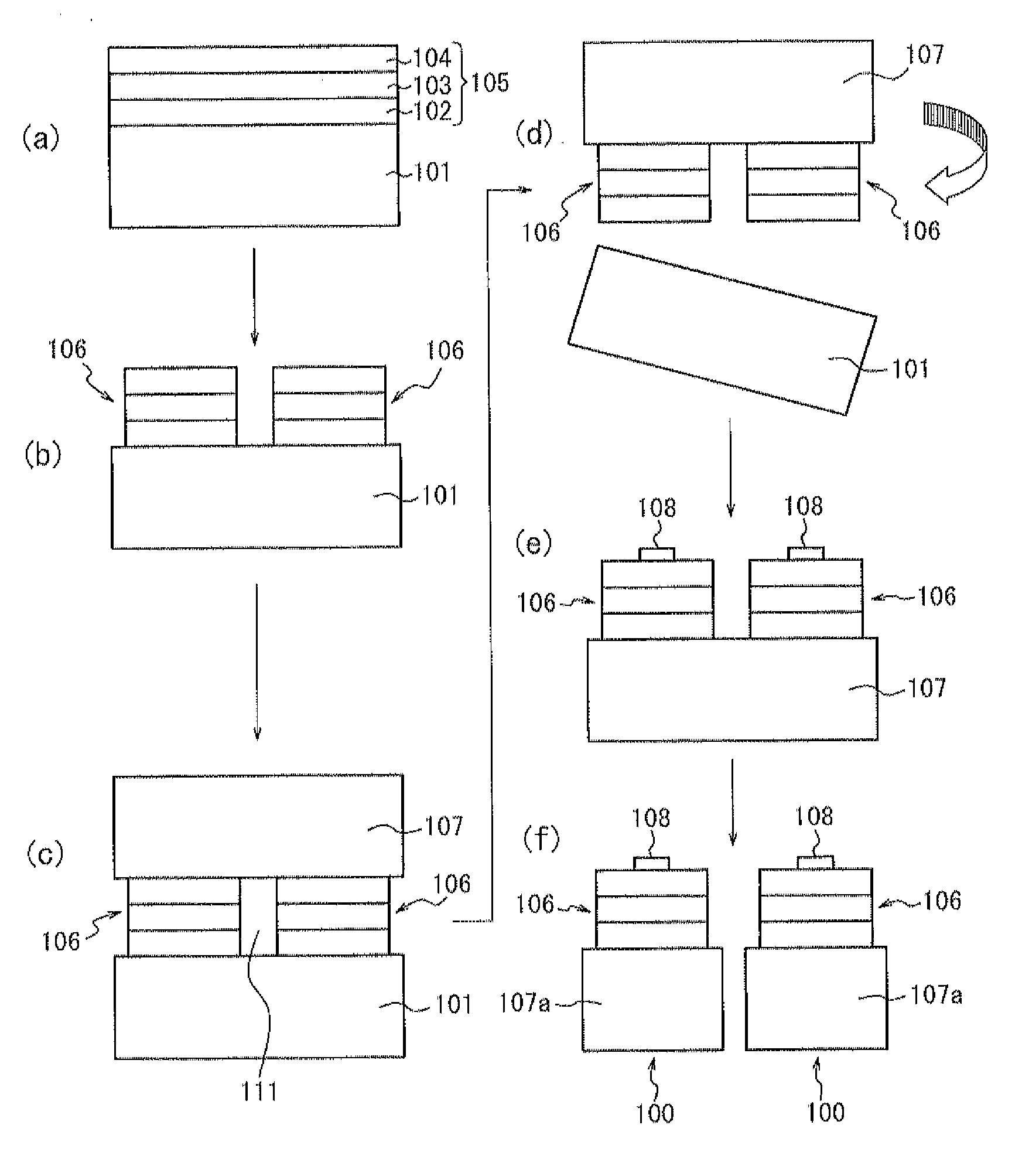
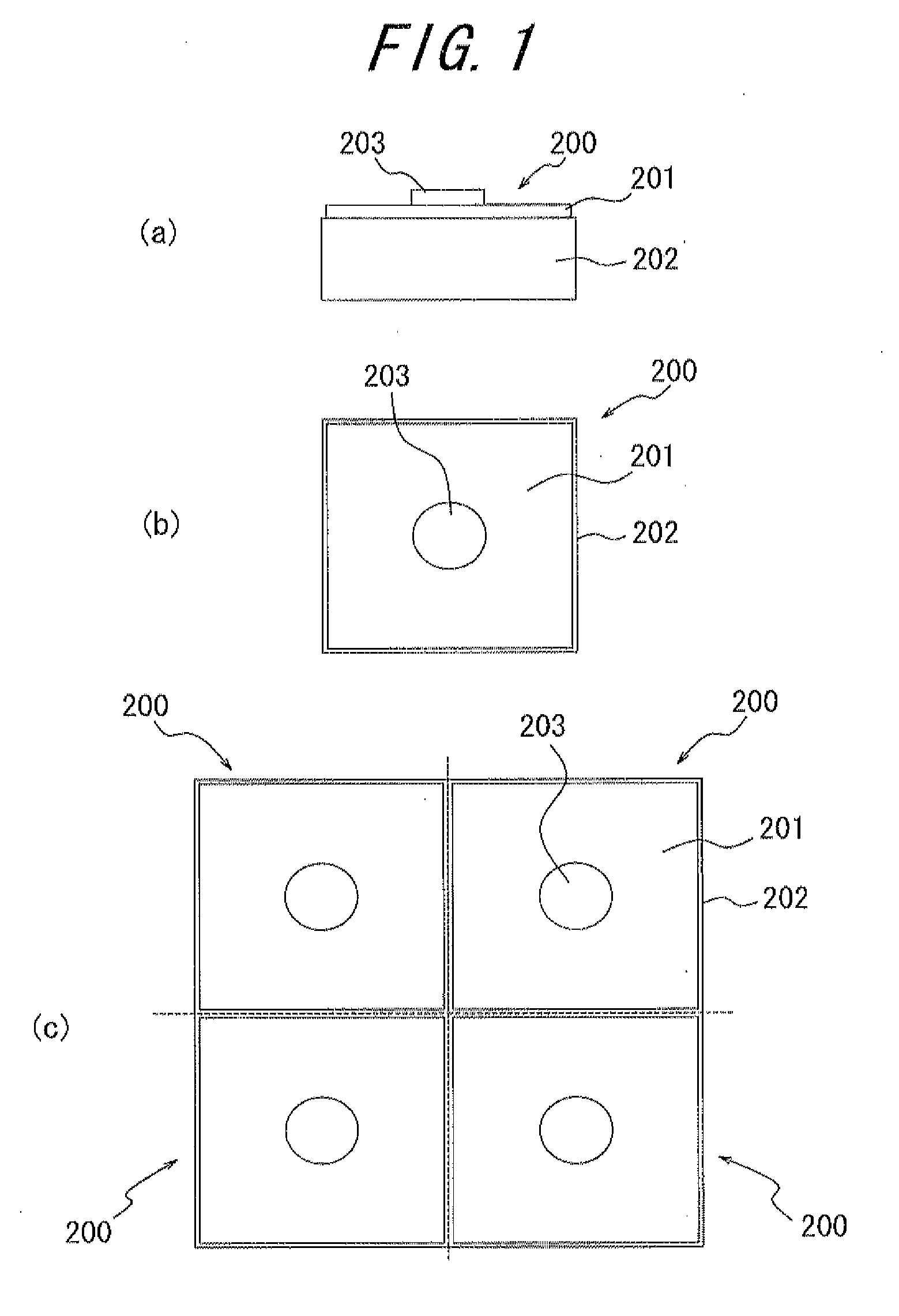
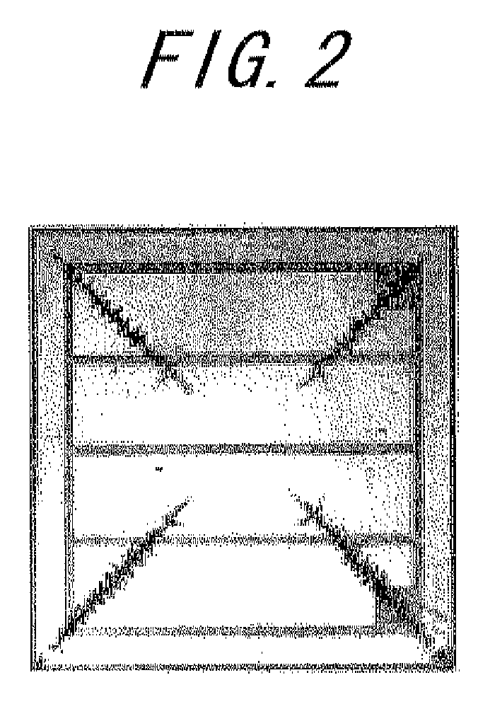
[0091]In Experimental Examples 1 to 8, a lift-off layer (CrN layer, thickness: 18 nm) was formed on a sapphire substrate, and then an n-type Group HI nitride semiconductor layer (GaN layer, thickness: 7 μm), a light emitting layer (InGaN-based MQW layer, thickness: 0.1 μm), and a p-type Group HI nitride semiconductor layer (GaN layer, thickness: 0.2 μm) were sequentially stacked to form a light emitting laminate. Subsequently, the light emitting laminate was partially removed to partially expose the sapphire substrate. Thus, a plurality of light emitting structures isolated like islands were formed such that the light emitting structures have a vertical cross section of a square, a square having rounded corners, or a circle. Table 1 shows the length L0 of a side of the square before rounding the corners, the curvature radius R, the length L1 of a straight portion in a side after the rounding, and the ratio of L1 to L0:L1 / L0.

TABLE 1Incidence ofIncidenceThr...

experimental examples 9 to 14

[0094]The sapphire substrate was separated by a similar method to the above Experimental Examples except for that the light emitting laminate was partially removed to form a plurality of light emitting structures isolated like islands such that the light emitting structures have a vertical cross-sectional shape of a regular octagon, a regular octagon having rounded corners, or a circle.

experimental examples 15 to 22

[0095]The sapphire substrate was separated by a similar method to the above Experimental Examples except for that the light emitting laminate was partially removed to form a plurality of light emitting structures isolated like islands such that the light emitting structures have a vertical cross-sectional shape of a regular dodecagon, a regular dodecagon having rounded corners, or a circle.


PUM


Abstract

A method for manufacturing vertically structured Group III nitride semiconductor LED chips includes a step of forming a light emitting laminate on a growth substrate; a step of forming a plurality of separate light emitting structures by partially removing the light emitting laminate to partially expose the growth substrate; a step of forming a conductive support on the plurality of light emitting structures; a step of lifting off the growth substrate from the plurality of light emitting structures; and a step of cutting the conductive support thereby singulating a plurality of LED chips each having the light emitting structure. The step of partially removing the light emitting laminate is performed such that each of the plurality of light emitting structures has a top view shape of a circle or a 4n-gon en” is a positive integer) having rounded corners.

Description

TECHNICAL FIELD[0001]The present invention relates to a vertically structured LED chip in which Group III nitride semiconductor layers are stacked, and a method for manufacturing the same.RELATED ART[0002]In general, Group III-V semiconductors made of compounds of Group III elements and Group V elements are widely used for devices such as light emitting diodes (LEDs).[0003]In manufacturing LEDs of a Group III-V semiconductor such as GaP, GaAs, AlGaAs, or AlInGaP, using Al, Ga, or In as a Group III element and using P or As as a Group V element, the semiconductor is grown on a single crystal substrate made of similar material to the semiconductor for the sake of lattice matching. For example, in cases of epitaxially growing AlGaAs, a GaAs substrate is typically used because AlGaAs is almost lattice matched to GaAs over the entire Al composition range.[0004]In bulk single crystal growth of GaP or GaAs, impurities are added for conductivity control to industrially produce high quality,...

Claims


Application Information

Patent Timeline
Patent Type & Authority Applications(United States)
IPC IPC(8): H01L33/40H01L33/08
CPCH01L33/0079H01L33/62H01L2933/0066H01L33/32H01L2924/0002H01L2924/00H01L33/0093H01L33/00H01L33/12
Inventor CHO, MEOUNG WHANLEE, SEOG WOOJANG, PIL GUKTOBA, RYUICHITOYOTA, TATSUNORIKADOWAKI, YOSHITAKA
Owner DOWA ELECTRONICS MATERIALS CO LTD
Why Eureka
Try Eureka