

Memory device and semiconductor device using the same
- Summary
- Abstract
- Description
- Claims
- Application Information
AI Technical Summary
Benefits of technology
Problems solved by technology
Method used
Image

Examples
embodiment 1
>
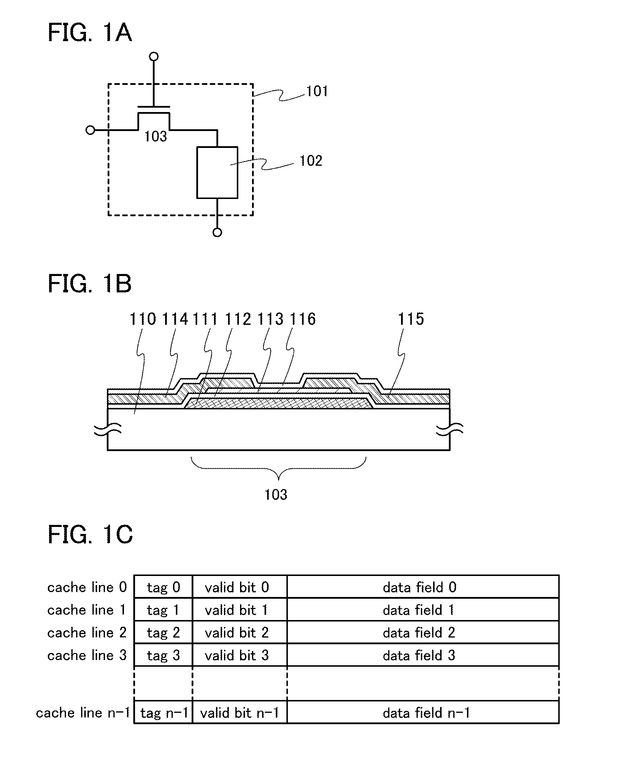
[0066]FIG. 1A is a circuit diagram illustrating a structure of a memory cell included in a memory device according to one embodiment of the present invention, as an example. In the circuit diagram illustrated in FIG. 1A, a memory cell 101 includes a memory element 102 and a transistor 103 which functions as a switching element. A semiconductor element such as a capacitor or a transistor can be used for the memory element 102. In the memory element 102, charge is accumulated in a capacitor or a gate capacitance formed between a gate electrode and an active layer of a transistor, whereby data is stored.
[0067]The transistor 103 functioning as a switching element controls supply of charge to the memory element 102, discharge of the charge from the memory element 102, and retention of the charge in the memory element 102.
[0068]Note that the memory cell 101 may further include another circuit element such as a transistor, a diode, a resistor, or an inductor as needed.
[0069]In one embodim...
embodiment 2
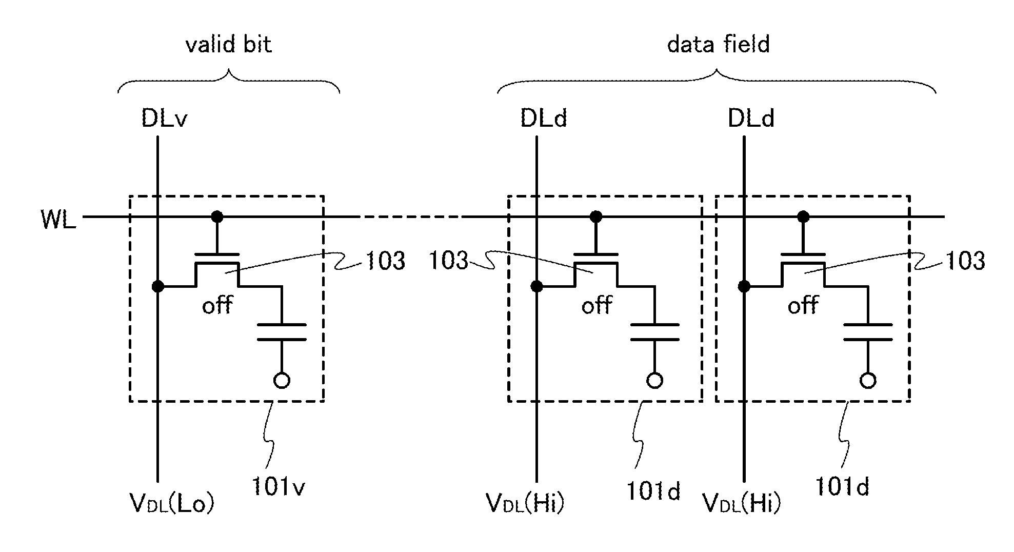
[0173]In this embodiment, examples of the structure of a memory device including a plurality of memory cells and a method for driving the memory device are described.
[0174]FIG. 11 is an example of a circuit diagram of a cell array 210 including the plurality of memory cells 101 one of which is illustrated in FIG. 3C. Unlike FIG. 3C, FIG. 11 illustrates an example of a circuit diagram in which a transistor 123 is a p-channel transistor.
[0175]In the cell array 210 illustrated in FIG. 11, a variety of wirings such as a plurality of first word lines WLa, a plurality of data lines DL, a plurality of second word lines WLb, and a plurality of source lines SL are provided, and a signal or a potential from a driver circuit is supplied to each of the memory cells 101 via the wirings. The source line SL is connected to a second terminal of the transistor 123.
[0176]Note that the number of the wirings can be determined by the number of the memory cells 101 and arrangement of the memory cells 101...
embodiment 3
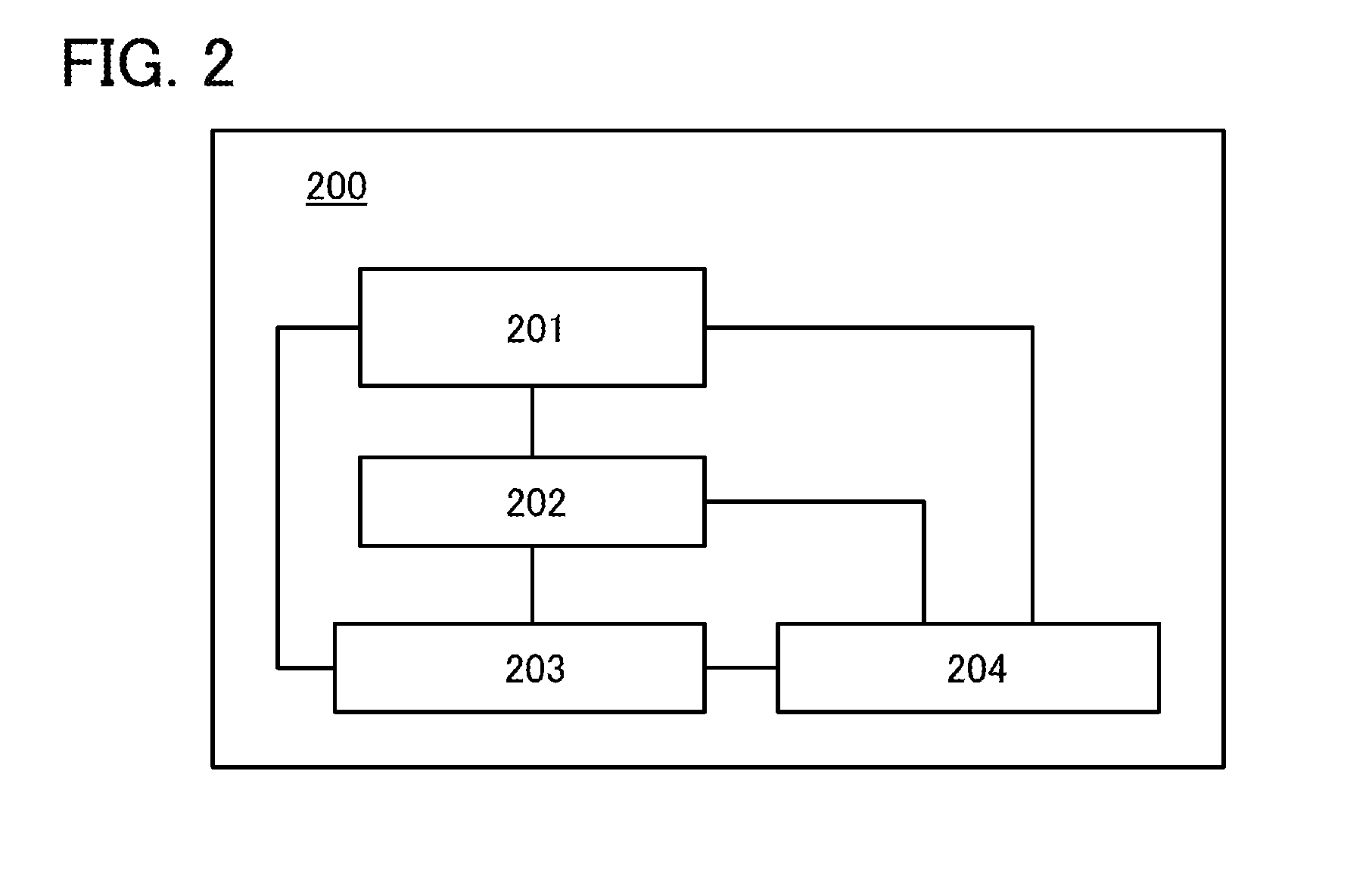
[0214]In this embodiment, a specific embodiment of a semiconductor device according to the present invention will be described. An example of the structure of the semiconductor device is illustrated as a block diagram in FIG. 14.
[0215]A semiconductor device 600 includes a control unit 601, an arithmetic logic unit (ALU) 602 corresponding to an arithmetic unit, a data cache 603, an instruction cache 604, a program counter 605, an instruction register 606, a main memory device 607, and a register file 608.
[0216]The control unit 601 has a function of decoding and carrying out an input instruction. The ALU 602 has a function of performing a variety of arithmetic operations such as four arithmetic operations and logic operations. The data cache 603 is a buffer memory device which temporary stores frequently used data. The instruction cache 604 is a buffer memory device which temporary stores frequently used instructions of instructions (programs) sent to the control unit 601. The program...
PUM
 Abstract
Description
Claims
Application Information