Check patentability & draft patents in minutes with Patsnap Eureka AI!

Photo detector consisting of tunneling field-effect transistors and the manufacturing method thereof

a tunneling field-effect transistor and photo detector technology, applied in the field of optical interconnection, can solve the problems of increasing power consumption, achieve the effects of reducing energy consumption, reducing required bias, and improving output current and sensitivity of the photo detector

Inactive Publication Date: 2012-10-18
FUDAN UNIV
View PDF3 Cites 3 Cited by
  • Summary
  • Abstract
  • Description
  • Claims
  • Application Information

AI Technical Summary

Benefits of technology

[0008]The present invention aims to provide a photo detector with low product energy consumption and fast response speed.
[0035]In this invention, the tunneling field-effect transistor (TFET) is integrated with the fiber, the TFET with the vertical channel is used as the photo detector to detect light, so the required bias is low, the energy consumption is reduced, and the output current and the sensitivity of the photo detector are improved. Meanwhile, the invention also adopts an autocollimation technology to manufacture the photo detector consisting of the TFET, so the process is more stable and the production cost is reduced.

Problems solved by technology

However, the thickening of the blocking layer influences the response speed of the photo detector to a large extent, and the p-i-n diode requires a higher bias to make ionizing collisions appear in the diode, so the power consumption is increased.

Method used


Image

  • Photo detector consisting of tunneling field-effect transistors and the manufacturing method thereof
  • Photo detector consisting of tunneling field-effect transistors and the manufacturing method thereof
  • Photo detector consisting of tunneling field-effect transistors and the manufacturing method thereof

Examples


Embodiment Construction

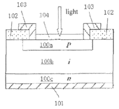
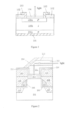
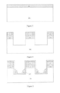
[0039]The invention is further described in detail by combining the attached drawings and the embodiments. In the figure, to facilitate description, the layer thickness and region thickness are amplified, but the sizes do not represent the actual dimensions. The figures fail to reflect the actual dimensions of the device accurately, but show the mutual positions of the regions and the structures, specifically the vertical and horizontal neighborhood of the structures.

[0040]The reference drawing provides schematic views of an ideal embodiment of the present invention. The embodiment of the present invention shall not be limited to the specific shapes of the regions as shown in the figure, but shall comprise all shapes, like deviations caused by manufacturing. For example, an etched curve is usually characterized by a bend or roundness and smoothness. But in this embodiment, all curves are represented by rectangles. The figure is schematic and shall not be considered as a limit of the...


PUM


Abstract

The present invention belongs to the technical field of optical interconnection and relates to a photo detector, in particular to a photo detector consisting of tunneling field-effect transistors.

Description

BACKGROUND OF THE INVENTION[0001]1. Technical Field[0002]The present invention belongs to the technical field of optical interconnection and relates to a photo detector, in particular to a photo detector consisting of tunneling field-effect transistors.[0003]2. Description of Related Art[0004]Compared with the traditional aluminum, copper has the following advantages: 1, the resistivity of copper is smaller (Cu: 1.7 μΩ / cm, Al: 3 μΩ / cm, the parasitic capacitance of the copper interconnection is smaller than that of the aluminum interconnection; 3, due to low resistance, the power consumption of the copper interconnection is smaller than that of the aluminum interconnection; 4, the electro-migration resistance of copper is better than that of aluminum (Cu<107 A / cm2, Al<106 A / cm2), connection cavities generated by electro-migration are avoided, so that the reliability of the device is improved. Therefore, devices adopting copper interconnections are able to meet the requirements ...

Claims


Application Information

Patent Timeline
Patent Type & Authority Applications(United States)
IPC IPC(8): H01L31/0368H01L31/18H01L31/0232
CPCG02B6/4214G02B6/42H01L31/1804H01L31/1136Y02E10/547H01L31/02327Y02P70/50H10K30/53H10B63/34H01L31/113
Inventor WANG, PENGFEILIN, XIWANG, WEILIU, XIAOYONGZHANG, WEI
Owner FUDAN UNIV
Features
  • R&D
  • Intellectual Property
  • Life Sciences
  • Materials
  • Tech Scout
  • Unparalleled Data Quality
  • Higher Quality Content
  • 60% Fewer Hallucinations
Learn More