Through silicon via processing techniques for lateral double-diffused mosfets

Active Publication Date: 2012-11-01
ALPHA & OMEGA SEMICON INC
View PDF3 Cites 39 Cited by
  • Summary
  • Abstract
  • Description
  • Claims
  • Application Information

AI Technical Summary

Benefits of technology

[0006]The present invention features a field effect transistor formed on a semiconductor substrate having formed thereon gate, source and drain regions, with the gate region having a lateral gate channel. A plurality of spaced-apart trenches or through semiconductor vias (TSV) each having an electrically conductive plug formed therein in electrical communication with the gate, source and drain regions

Problems solved by technology

However it is difficult to route the source of an LDMOS trans

Method used


Image

  • Through silicon via processing techniques for lateral double-diffused mosfets
  • Through silicon via processing techniques for lateral double-diffused mosfets
  • Through silicon via processing techniques for lateral double-diffused mosfets

Examples


Embodiment Construction

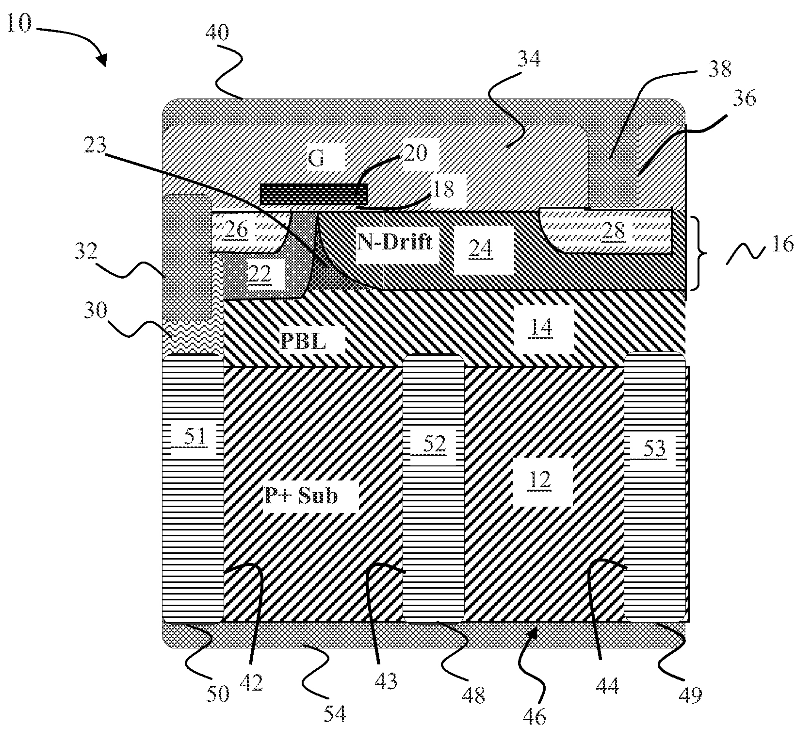
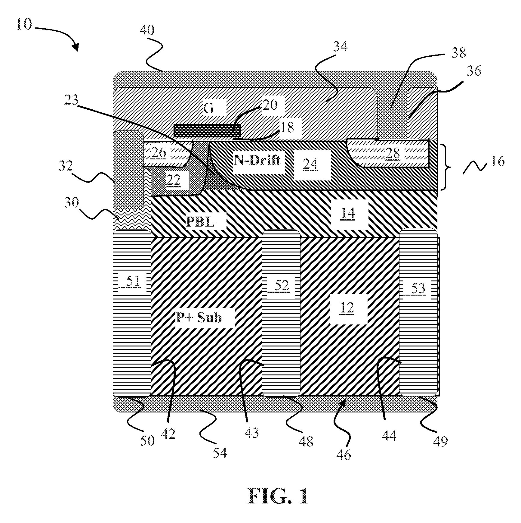
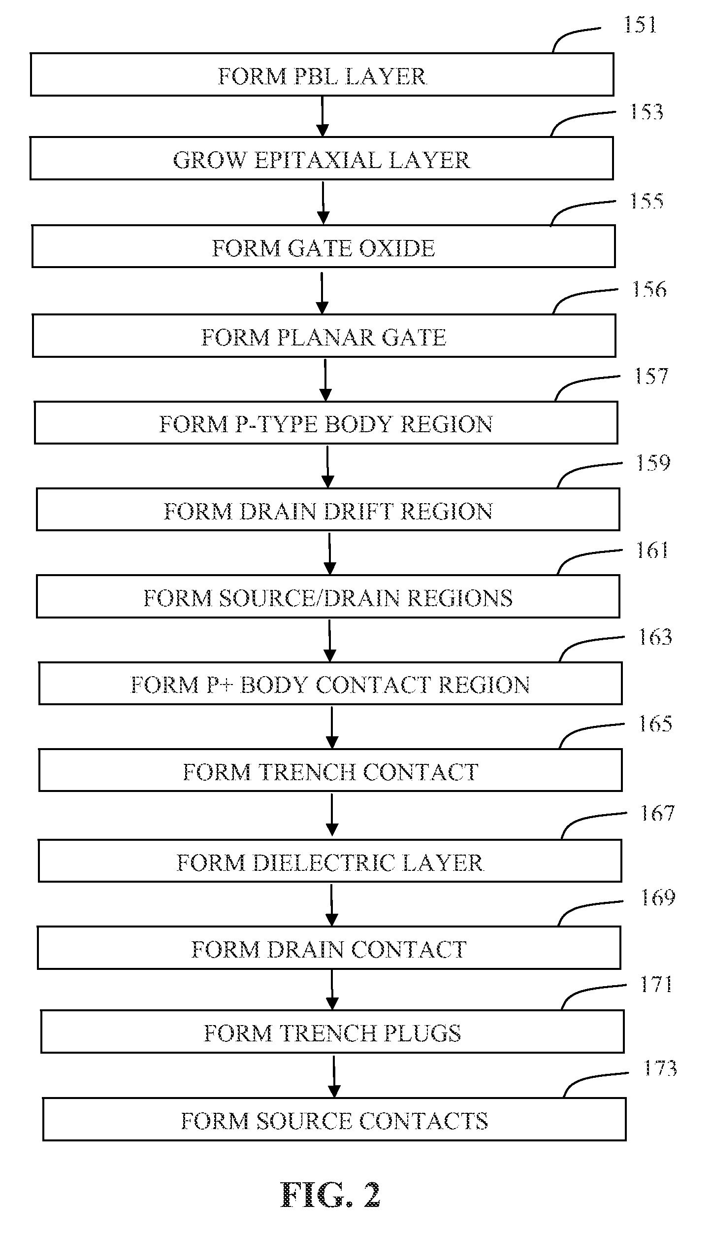
[0020]Referring to both FIGS. 1 and 2, LDMOS 10 is formed on a P-type substrate 12 with an epitaxial layer 16 is formed thereon, A P-type buried layer (PBL) 14 is formed at the junction of the P-type stibstrate 12 and the epitaxial layer 16 as indicated at step 151, The epitaxial layer 16 is grown on top of the PBL layer as indicated at step 153. The epitaxial layer may be N-type or P-type. The active regions of transistor 10 are formed in the epitaxial layer 16. PBL 14 may be formed by standard buried layer implantation processes, or alternatively, may be formed using a step epitaxial process. That is, a heavily doped P-type epitaxial layer may be grown on top of substrate 12 to serve as PBL 14. Alternatively, the PBL 14 may be formed by deep implantation. Epitaxial layer 16 may be grown on top of the PBL 14. A thickness of PBL layer 14 may be about couple of microns thick when a thickness of epitaxial layer 16 is in a range of few microns to 10 microns. Specifically, epitaxial lay...


PUM


Abstract

The present invention features a field effect transistor forming on a semiconductor substrate having formed thereon gate, source and drain regions, with said gate region having a lateral gate channel. A plurality of spaced-apart trenches each having an electrically conductive plug formed therein in electrical communication with said gate, source and drain regions, with said trenches extend from a back surface of said semiconductor substrate to a controlled depth. A trench contact shorts the source region and a body region. A source contact is in electrical communication with said source region and a drain contact in electrical communication with said drain region, with said source and drain contacts being disposed on opposite sides of said gate channel.

Description

BACKGROUND OF THE INVENTION[0001]The invention relates to high voltage semiconductor devices and the manufacturing process thereof and, in particular, to a lateral double-diffused metal oxide semiconductor (LDMOS) transistor, particularly to vertical discrete LDMOS with source on the device backside. The device is considered ‘vertical’ because the source is on the bottom and the drain is on the top (or vice-versa). The term ‘lateral’ refers to the planar gate of the device.[0002]Lateral double-diffused metal-oxide-semiconductor (LDMOS) transistors are commonly used in high-voltage applications (e.g. 20 to 500 volts or higher) because of their high breakdown voltage characteristics and compatibility with complementary metal—oxide—semiconductor (CMOS) technology for low voltage devices. In general, an LDMOS transistor includes a planar polysilicon gate, an N+ source region formed in a P-type body region, and an N+ drain region. The N+ drain region is separated from the channel formed ...

Claims


Application Information

Patent Timeline
IPC IPC(8): H01L29/78H01L21/336
CPCH01L29/0634H01L29/66681H01L29/1083H01L29/4175H01L29/41766H01L29/456H01L29/66659H01L29/78H01L29/782H01L29/7835H01L29/7839H01L23/49562H01L23/49575H01L21/743H01L21/76898H01L2924/0002H01L29/0878H01L29/1095H01L21/76879H01L2924/00H01L29/402
Inventor MALLIKARJUNASWAMY, SHEKAR
Owner ALPHA & OMEGA SEMICON INC
Why Eureka
Try Eureka