Method and products related to deposited particles

a technology of deposited particles and deposited particles, which is applied in the field of encapsulated particles, can solve the problems of difficult curvature required for the efficient removal of encapsulant, expensive equipment and a controlled environment, and the cost of process stage of integrated silicon based microchips or other discrete components with printed circuitry (antenna), and achieve good electrical and mechanical contact of components to the substra

Inactive Publication Date: 2012-11-01
TEKNOLOGIAN TUTKIMUSKESKUS VTT
View PDF3 Cites 14 Cited by
  • Summary
  • Abstract
  • Description
  • Claims
  • Application Information

AI Technical Summary

Benefits of technology

[0019]The invention also presents a related processing method, where even large-scale circuits can be fabricated on low-cost substrates by drop-on-demand printing (digitally defined print pattern) and chip-on-demand placing (various different components places at digitally defined component locations with respect to the printed electrodes).
[0020]According to one embodiment, a topmost substrate layer capable of removing the encapsulating material as the ink solvent is absorbed is used for connecting one or more discrete electrical components to the substrate. The ink / paste particles with the encapsulating material removed when deposited on the solvent-absorbing surface provide good electrical and mechanical contacting of the component to the substrate.

Problems solved by technology

Therefore, the curing temperature required for the efficient removal of the encapsulant is often challenged by the thermal tolerance of the substrate.
This is a problem frequently encountered when attempting to form metallic conductors on flexible substrates by means of printing a dispersion of encapsulated metallic nanoparticles followed by thermal curing to remove the encapsulant to enable sintering.
All known sintering methods have their advantages but they also suffer from certain disadvantages.
The printing of devices and circuit components is still at a technology development stage: process related limitations (e.g. the minimum gap spacing between printed conductors) as much as material limitations (e.g. the stability and mobility of organic semiconductors) persist regardless of the efforts of the scientific community and industry.
Apparently, some pioneered printed electronics processing lines are capable of all-printing fully functional RFID tags, but these typically require expensive equipment and a controlled environment.
More mature technologies such as screen printing of silver paste for antenna fabrication have proven competitive, though the integration of the silicon based microchip, or other discrete components, with the printed circuitry (antenna) is a costly process stage.
The generic problem with interconnecting components to the printed circuitry is how to deliver a discrete component to the precise location (aligned to the printed contact pads) in a high throughput manner.
An additional challenge related to flip-chip bonding to (nanoparticle ink) inkjet printed and sintered wiring is the electrically insulating layer that tends to form on the top surface of the sintered conductor.

Method used


Image

  • Method and products related to deposited particles
  • Method and products related to deposited particles
  • Method and products related to deposited particles

Examples


examples

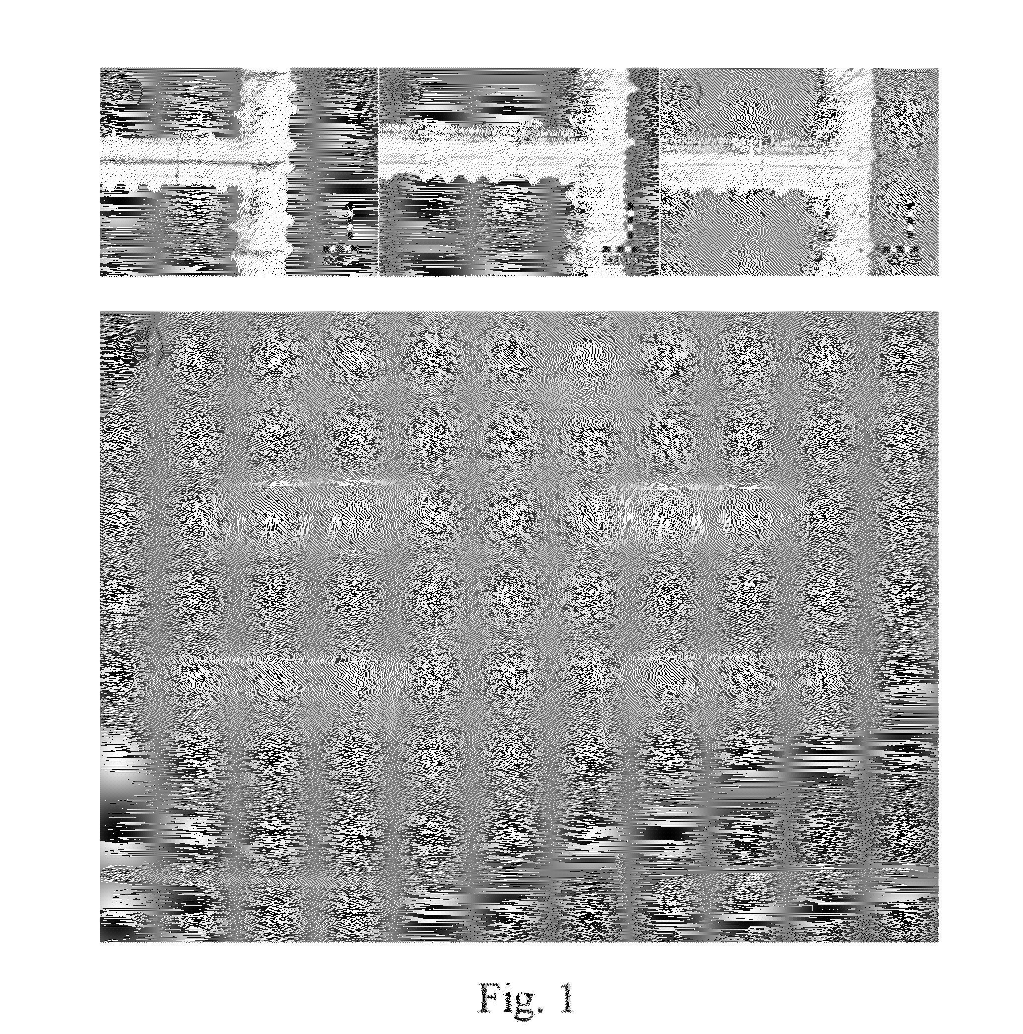
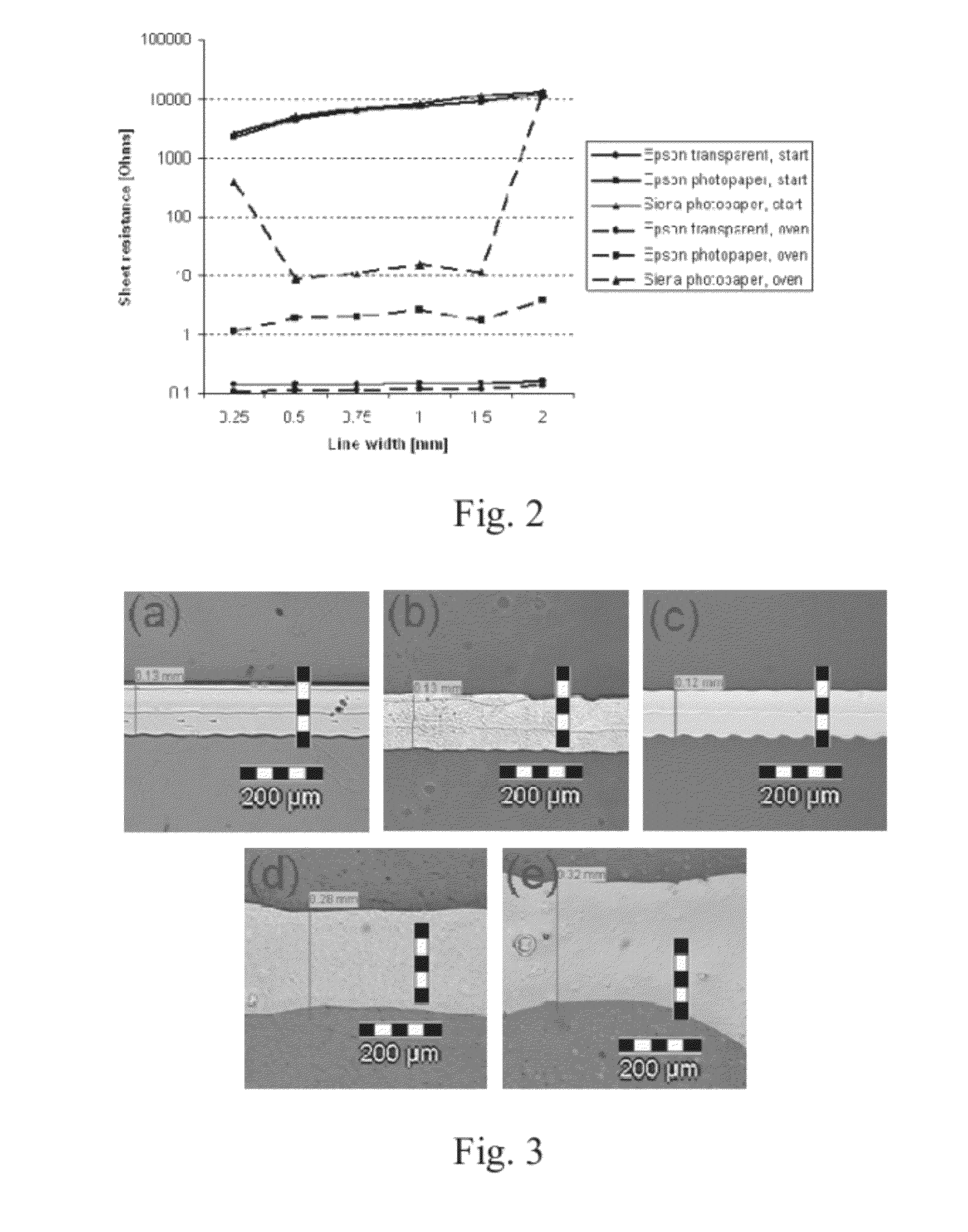
[0072]The following examples demonstrate the invention with suitable commercially available nanoparticle inks and coated substrates.

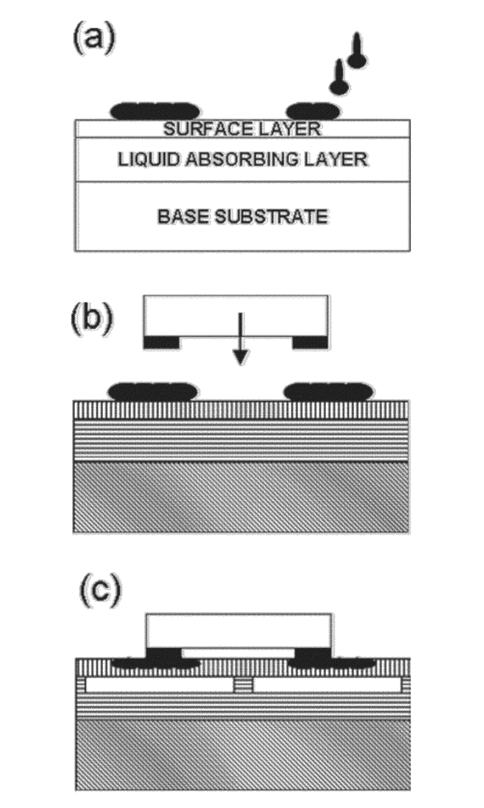
[0073]Since inkjet printing substrates are engineered to provide fixation of the inks on the substrates, one could expect to have strong fixation also for some metallic nanoparticle ink formulations. For pigmented inks, fixation is obtained by the chemical reaction between the pigment coating and the surface layer of the substrate in a self-fixing manner. For the substrate facilitated removal of the encapsulating material of printed electronics inks / pastes, the affinity of the printing substrate for the capping material should be so strong as to break the encapsulating molecule—particle core bonds and release the particle cores into physical contact.

[0074]The results of the example tests presented here were conducted with Advanced Nano Products DGP-45LT-15C ink, which consists of silver nanoparticles with a nominal particle size of 10-20 nm and a trieth...


PUM

PropertyMeasurementUnit
sizeaaaaaaaaaa
sizeaaaaaaaaaa
diameteraaaaaaaaaa

Abstract

The invention concerns a method of removing encapsulating material from encapsulated particles deposited onto a substrate. According to the method, a substrate is used which is capable of facilitating said removal of encapsulating material. The particles may be nanoparticles. In particular, the substrate-facilitated removal may result in sintering of the particles. The invention provides a novel way of functionalizing electronic structures using particulate matter and for conveniently producing e.g. printed electronics devices.

Description

FIELD OF THE INVENTION[0001]The invention relates to encapsulated particles deposited on substrates for example for the purposes of printed electronics. In particular, the invention relates to a method of efficiently removing the encapsulating material covering metallic, metal oxide and semiconductor particles deposited on substrates for the purpose of forming functionalized structures. Also, the invention relates to products enabled by removing the encapsulating material and apparatuses suitable for this purpose. The invention provides a method for producing conductors by depositing encapsulated metallic particles on substrates and removing the encapsulating material to enable sintering. The invention provides a method for interconnecting discrete components to the sintered structure. In addition, the invention relates to products produced by sintering and interconnecting of discrete components to the sintered structure.BACKGROUND OF THE INVENTION[0002]Printed electronic components...

Claims


Application Information

Patent Timeline
Patent Type & Authority Applications(United States)
IPC IPC(8): B05D5/12H05K7/00H05K3/30C11D7/60H05K3/00B82Y30/00B82Y40/00
CPCB82Y30/00C09D11/52H05K1/038H05K3/12H05K3/125H05K3/1283Y10T29/4913H05K3/38H05K2201/0116H05K2201/0209H05K2201/0284H05K2201/10106H05K2201/10636H05K3/32Y02P70/50C09D11/00H05K13/00
Inventor ALLEN, MARKLEPPANIEMI, JAAKKOMATTILA, TOMI
Owner TEKNOLOGIAN TUTKIMUSKESKUS VTT
Why Eureka
Try Eureka