Micromechanical Method and Corresponding Assembly for Bonding Semiconductor Substrates and Correspondingly Bonded Semiconductor Chip

a micromechanical and semiconductor chip technology, applied in semiconductor devices, semiconductor/solid-state device details, electrical apparatus, etc., can solve the problems of inconsiderable area requirement, liquid eutectic phase flowing into mems functional regions in an uncontrolled manner,

Inactive Publication Date: 2012-11-08
ROBERT BOSCH GMBH
View PDF1 Cites 10 Cited by
  • Summary
  • Abstract
  • Description
  • Claims
  • Application Information

AI Technical Summary

Problems solved by technology

In this case, it can happen that the liquid eutectic phase flows into MEMS functional regions in an uncontrolled manner.
As a result, an inconsiderable area requirement is necessary precisely in the case of sensor chips that are becoming ever smaller.

Method used


Image

  • Micromechanical Method and Corresponding Assembly for Bonding Semiconductor Substrates and Correspondingly Bonded Semiconductor Chip
  • Micromechanical Method and Corresponding Assembly for Bonding Semiconductor Substrates and Correspondingly Bonded Semiconductor Chip
  • Micromechanical Method and Corresponding Assembly for Bonding Semiconductor Substrates and Correspondingly Bonded Semiconductor Chip

Examples


first embodiment

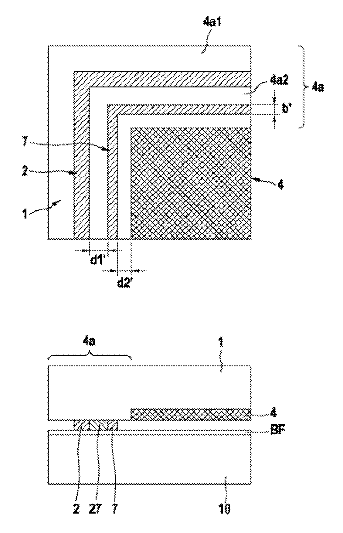
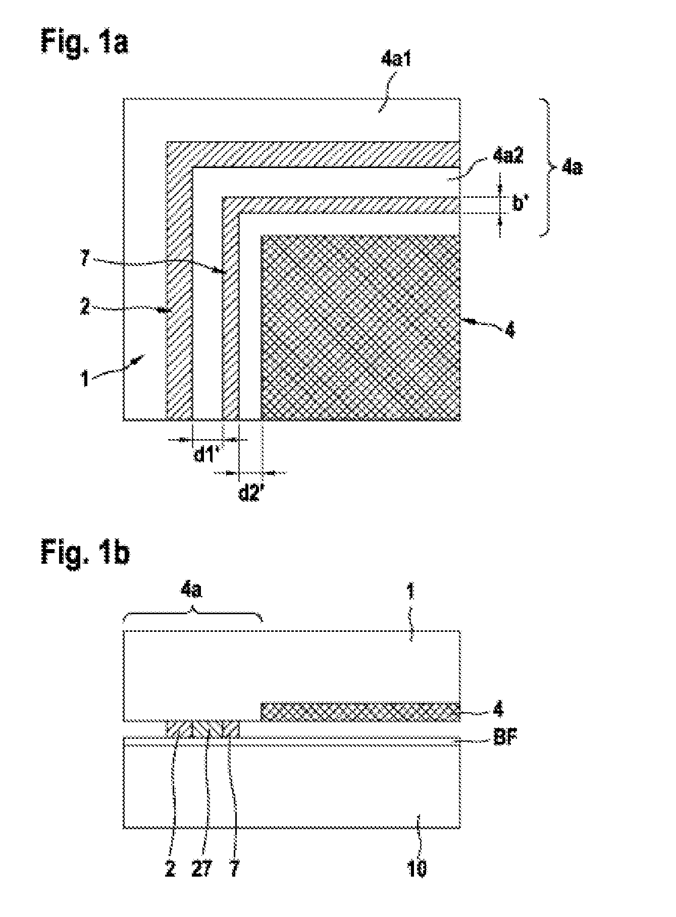
[0024]FIG. 1a is a schematic partial plan view of a chip region of an assembly for bonding semiconductor substrates in accordance with the present invention.

[0025]The micromechanical sensor chip 1, which has an active functional region 4 and a passive edge region 4a. Provided in the edge region 4a is a bonding frame 2 with an applied eutectic bonding alloy, for example Al—Ge, which splits the edge region 4a into an inner region 4a2, which is surrounded by the bonding frame, and an outer region 4a1. A stop frame 7 is arranged in the inner region 4a2 between bonding frame 2 and functional region 4 of the sensor chip 1, said stop frame consisting of a non-eutectic alloy composed of Al and Ge, that is to say having either a higher Ge content or a higher Al content (up to the respective pure alloy component) than the corresponding eutectic alloy.

[0026]This additionally provided stop frame 7, upon contact with the flow movement (proceeding from the bonding frame 2) of the eutectic melt pr...

second embodiment

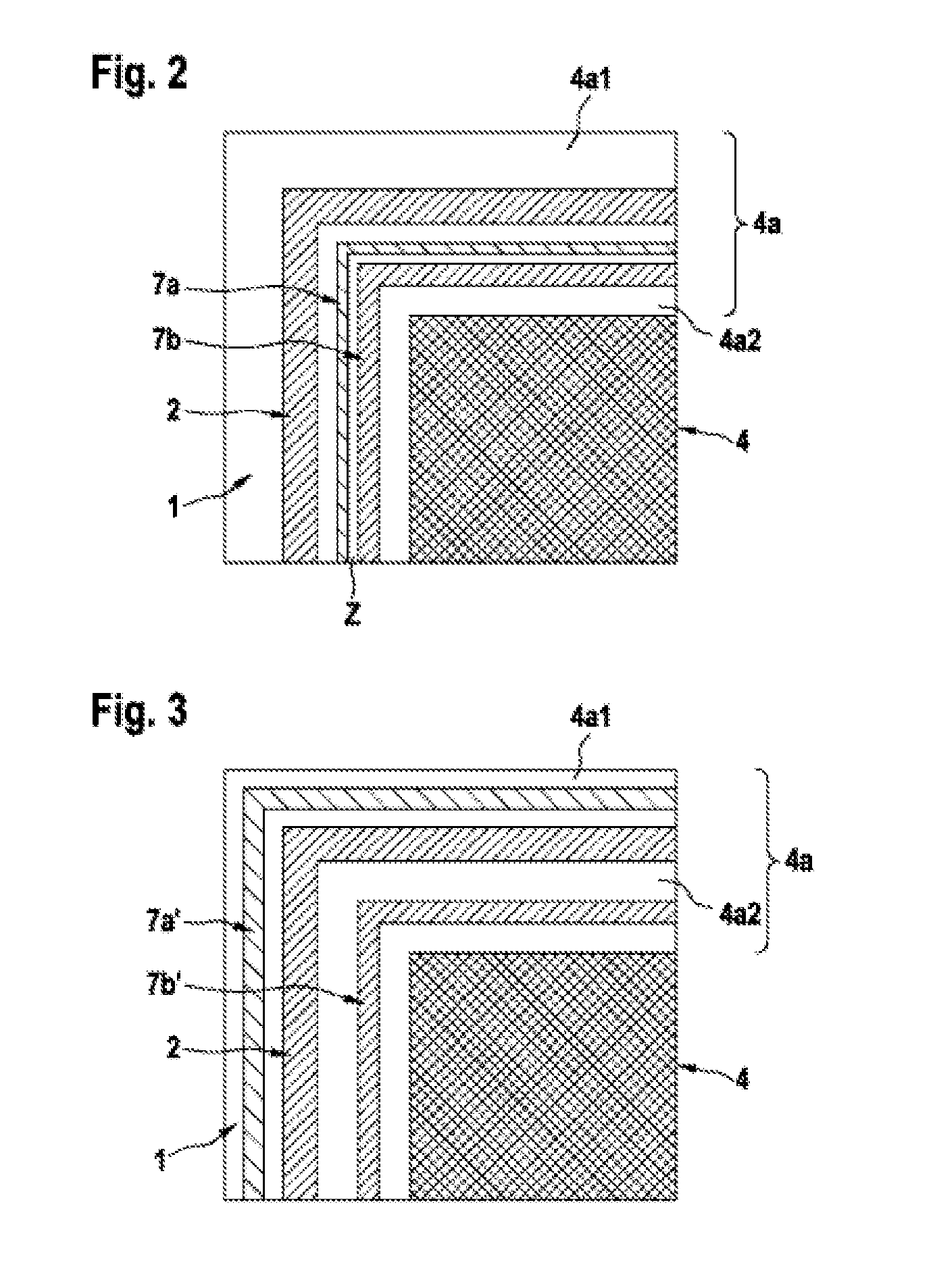
[0030]FIG. 2 is a schematic partial plan view of a chip region of an assembly for bonding semiconductor substrates in accordance with the present invention.

[0031]In the case of the second embodiment in accordance with FIG. 2, a double stop frame 7a, 7b with an interspace Z situated between the two stop frames 7a, 7b is provided. In the case of this second embodiment, in addition to altering the mixing ratio of the alloy out of the eutectic range, it is possible to utilize the capillary effect that forms between the two stop frames 7a, 7b, which are led in a parallel fashion, in the interspace Z. As a result of this capillary effect, relatively large amounts of a eutectic melt which occur locally can be rapidly distributed along the stop frames 7a, 7b by way of the interspace Z. This rapid distribution provides for the supply of a substantial amount of contact with the material of the stop frames, which accelerates the solidification, in order thus to be able to prevent even more eff...

third embodiment

[0033]FIG. 3 is a schematic partial plan view of a chip region of an assembly for bonding semiconductor substrates in accordance with the present invention.

[0034]In the case of the third embodiment in accordance with FIG. 3, a respective stop frame 7a′ and 7b′ composed of a non-eutectic alloy or one of the alloy components are provided both outside the bonding frame 2 and within the bonding frame 2.

[0035]Otherwise, the third embodiment corresponds to the first and second embodiments.


PUM


Abstract

A micromechanical assembly for bonding semiconductor substrates includes a semiconductor substrate having a chip pattern having a plurality of semiconductor chips, each having a functional region and an edge region surrounding the functional region. There is a bonding frame made of a bonding alloy made from at least two alloy components in the edge region, spaced apart from the functional region. Within the part of the edge region surrounding the bonding frame between the bonding frame and the functional region, there is at least one stop frame made of at least one of the alloy components, which is configured such that when a melt of the bond alloy contacts the stop frame during bonding, the bonding alloy solidifies.

Description

PRIOR ART[0001]The present invention relates to a micromechanical method and a corresponding assembly for bonding semiconductor substrates and a corresponding bonded semiconductor chip.[0002]Although applicable to any micromechanical components and structures, in particular sensors and actuators, the present invention and the problem area addressed thereby will be explained with regard to a micromechanical sensor that can be produced using the technology of silicon surface micromachining.[0003]Micromechanical substrate connections, e.g. wafer-wafer bonding connections, are usually realized by eutectic alloys comprising two or more solid bonding materials or alloy components as constituents. Eutectic alloys of this type have an unambiguously determinable melting point. By contrast, other mixing ratios with the same alloy components have a melting or solidification range in which, alongside the melt, a solid phase is also present. The melting point of the eutectic alloy is, moreover, ...

Claims


Application Information

Patent Timeline
Patent Type & Authority Applications(United States)
IPC IPC(8): H01L23/48H01L21/30
CPCB81C1/00269H01L2924/1461B81C2203/0118B81C2203/019B81C2203/036H01L23/10H01L24/29H01L24/30H01L24/32H01L24/83H01L25/50H01L2224/26145H01L2224/29011H01L2224/29013H01L2224/29076H01L2224/29078H01L2224/291H01L2224/29117H01L2224/29124H01L2224/30051H01L2224/30131H01L2224/30135H01L2224/30177H01L2224/30505H01L2224/30515H01L2224/32054H01L2224/32145H01L2224/32501H01L2224/83007H01L2224/83095H01L2224/83191H01L2224/83365H01L2224/83815H01L2924/01013H01L2924/01029H01L2924/01032H01L2924/0105H01L2924/01079H01L2924/01082H01L2924/1631H01L2924/165B81C2201/019H01L2224/29144H01L2224/29109H01L2924/01005H01L2924/01006H01L2924/01033H01L2924/01322H01L2924/014H01L2224/29101H01L2924/0132H01L2224/29111H01L2924/00H01L2924/01014H01L2924/01049H01L2924/00014
Inventor TRAUTMANN, ACHIMREICHENBACH, RALF
Owner ROBERT BOSCH GMBH
Why Eureka
Try Eureka