Pressure sensor

a technology of pressure sensor and mos structure, which is applied in the direction of fluid pressure measurement, fluid pressure measurement by electric/magnetic elements, instruments, etc., can solve the problems of reducing the performance of the n-channel mos structure and excessive well-being, so as to reduce the desiccated space of the signal processing circuit and improve the effect of performan

Inactive Publication Date: 2012-11-15
NIIMURA YUICHI +3
View PDF9 Cites 4 Cited by
  • Summary
  • Abstract
  • Description
  • Claims
  • Application Information

AI Technical Summary

Benefits of technology

[0007]In view of the above, the present invention provides a pressure sensor capable of reducing a desiccated space of a signal processing circuit in a semiconductor substrate, and improving performance.
[0009]With the above configuration, the signal processing circuit is formed in the p-type conductive region formed at the surface around the diaphragm in the semiconductor substrate, and the n-type conductive region is formed in the p-type conductive region by diffusion of n-type impurities. Further, the piezo resistive element is formed by diffusion of p-type impurities into the n-type conductive region. Therefore, the dedicated space of the signal processing circuit in the semiconductor substrate can be reduced and the performance can be improved, compared to the prior art in which both of the piezo resistive element and the signal processing circuit are installed in the n-type conductive region.
[0013]Accordingly, the sensitivity decrease of the pressure conversion unit due to the thin film layer can be further suppressed.
[0015]With such configuration, the stress applied to the protective film can be offset by the stress of the stress control film.
[0017]Accordingly, the conductive thin film layer serves as a shield and thus can reduce the resistance change of the piezo resistive element which is caused by the external electric field.
[0020]With such configuration, the effect of the resistance change of the portions that does not include the piezo resistive element can be reduced, and thereby the detection accuracy can be increased.

Problems solved by technology

Or, when the p well region is formed in the n-type epitaxial silicon layer, the concentration of the p well is excessively increased and, thus, the performance of the n-channel MOS structure is lowered.

Method used


Image

  • Pressure sensor
  • Pressure sensor
  • Pressure sensor

Examples


first embodiment

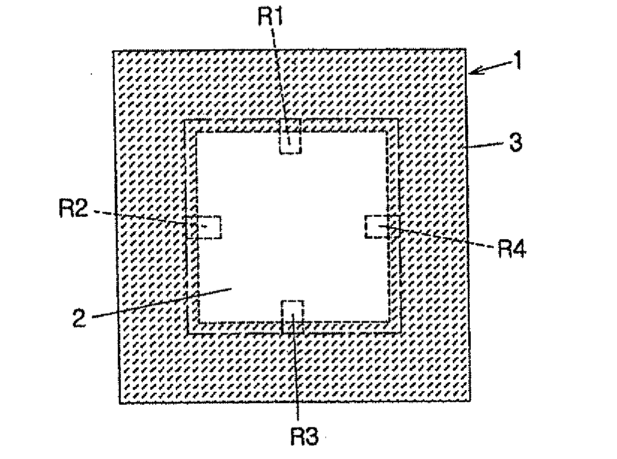
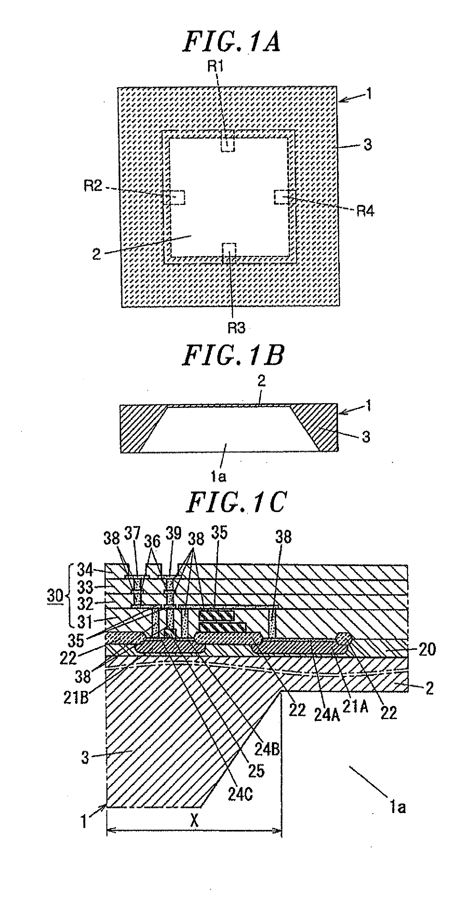
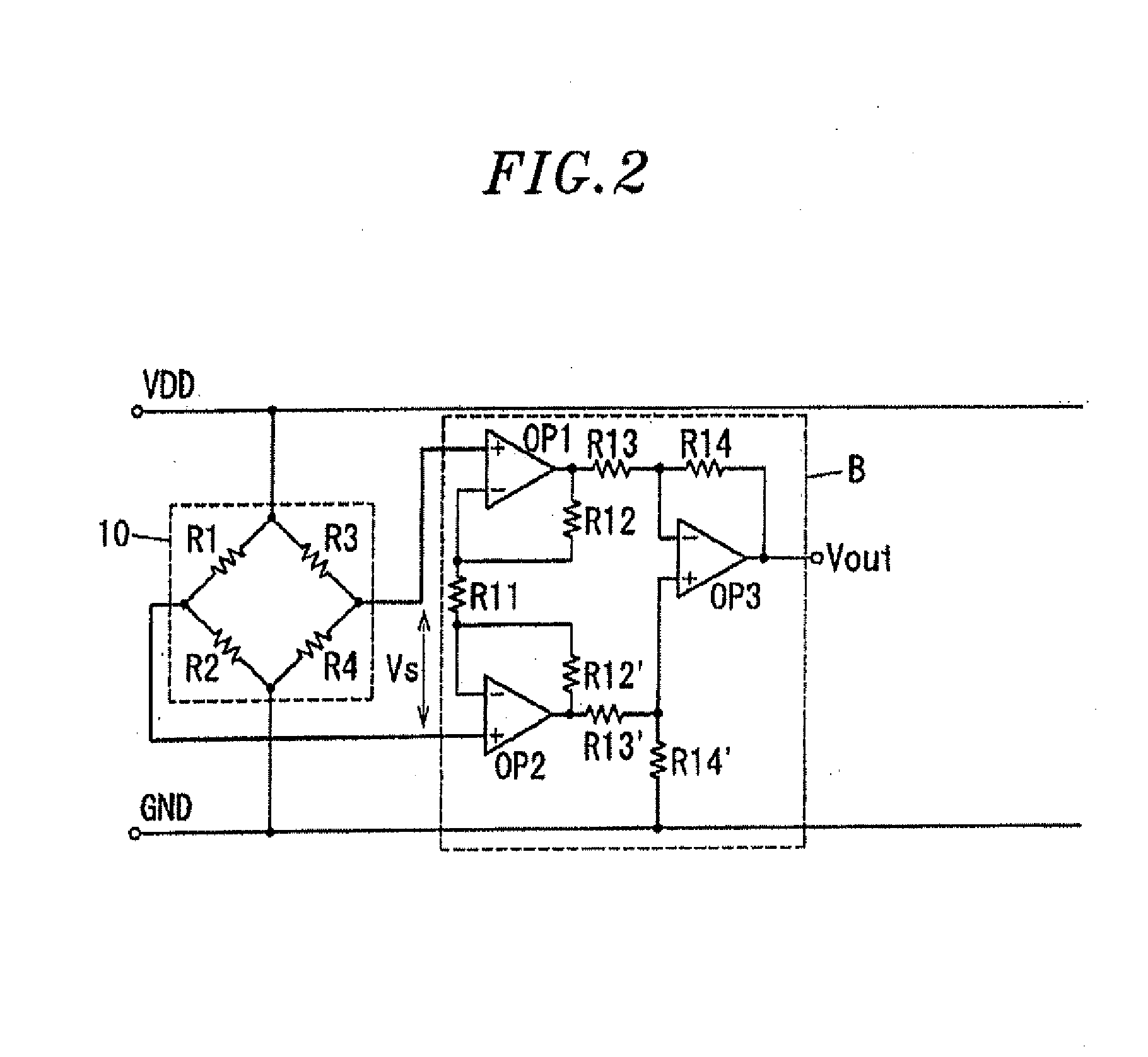
[0033]FIG. 1A shows a top view of a pressure sensor of the present embodiment; FIG. 1B illustrates a cross sectional view thereof; and FIG. 1C depicts a cross sectional view showing principal parts thereof. The pressure sensor includes a pressure conversion unit 10 (see FIG. 2) in which four piezo resistive elements (hereinafter, simply referred to as “piezo resistors”) R1 to R4 are formed on a main surface side (top surface side in FIG. 1B) of a diaphragm 2 provided in a semiconductor substrate 1, e.g., a single crystalline silicon substrate.

[0034]The diaphragm 2 is provided by forming a recess 1a having a substantially truncated pyramid shape when seen from a side surface on a backside of the semiconductor substrate 1 (bottom surface side in FIG. 1B) by using an anisotropic etching technique or the like. Hereinafter, a peripheral portion around the diaphragm 2 having a uniform thickness is referred to as a frame 3 in the semiconductor substrate 1.

[0035]The four piezo resistors R1 ...

second embodiment

[0047]In the first embodiment, the thin film layer 30 is formed on the entire main surface side of the semiconductor substrate 1 including the diaphragm 2. In that case, the following problems may be generated.

[0048]1) Since the substantial thickness of the diaphragm 2 is increased by the thin film layer 30, the diaphragm 2 is not easily bent and this results in decrease of the detection accuracy.

[0049]2) Since the thin film layer 30 is formed on the piezo resistor Ri such that the piezo resistor Ri is disposed near the middle of the pressure sensor in the thickness direction, the piezo resistor Ri is less bent even by the same pressure compared to the piezo resistor Ri positioned at the surface of the pressure sensor, which deteriorates the detection sensitivity.

[0050]3) When the pressure is not applied from the outside, the diaphragm 2 may be bent by any internal stress of the thin film layer 30. This results in a great offset in the output voltage Vs of the pressure conversion un...

third embodiment

[0054]In the second embodiment, among the thin film layer 30 formed on the main surface side of the diaphragm 2, the portion of the thin film layer 30 where the piezo resistors Ri are not formed below has been removed. On the other hand, in the present embodiment, the portion of the thin film layer 30 where the piezo resistors Ri are formed below (the portions indicated by oblique lines in FIG. 4A) is also partially removed on the main surface side of the diaphragm 2, as shown in FIG. 4.

[0055]By further removing the thin film layer 30 where the piezo resistors Ri are formed below as described above, the above-described problems 1) and 2) can be further improved. In that case, it is preferable to protect the diaphragm 2, the piezo resistors and the cross section of the thin film layer 30 electrically, chemically and physically, by covering them with a protective film 40 formed of an insulating thin film (oxide film) (see FIGS. 4B and 4C).


PUM

PropertyMeasurementUnit
pressureaaaaaaaaaa
p-type conductiveaaaaaaaaaa
n-type conductiveaaaaaaaaaa

Abstract

A pressure sensor includes: a pressure conversion unit and a signal processing circuit installed in a semiconductor substrate. The pressure conversion unit includes: a diaphragm formed by partially thinning the semiconductor substrate; and a plurality of piezo resistive elements formed on a surface of the diaphragm. The signal processing circuit is constituted by a complementary metal-oxide semiconductor (CMOS) integrated circuit formed in a p-type conductive region disposed around the diaphragm on the surface of the semiconductor substrate, and the piezo resistive elements are provided by forming an n-type conductive region in the p-type conductive region on the surface of the diaphragm by diffusion of n-type impurities and diffusing p-type impurities in the n-type conductive region.

Description

FIELD OF THE INVENTION[0001]The present invention relates to a pressure sensor; and, more particularly, to a pressure sensor in which a pressure conversion unit for converting a pressure to an electrical signal and a signal processing circuit for processing the electrical signal obtained by the pressure conversion unit are formed as a single semiconductor substrate.BACKGROUND OF THE INVENTION[0002]Conventionally, there are provided various pressure sensors in which a pressure conversion unit consisting of a diaphragm and a piezo resistive element and a signal processing circuit for processing an electrical signal obtained by the pressure conversion unit are installed in a single semiconductor substrate.[0003]For example, in a pressure sensor described in Patent Document 1, a diaphragm and a piezo resistive element are formed in a single crystalline silicon substrate, and a signal processing circuit is installed around the diaphragm. In the related prior art, a manufacturing cost can...

Claims


Application Information

Patent Timeline
Patent Type & Authority Applications(United States)
IPC IPC(8): G01L9/06
CPCG01L9/0042G01L9/0054H01L27/0629G01L9/0055G01L9/00H01L29/84
Inventor NIIMURA, YUICHINOBE, TAKESHINISIKAWA, HIDEOKATO, FUMIHITO
Owner NIIMURA YUICHI
Why Eureka
Try Eureka