Dual pass scanning

a lithography apparatus and chargeless technology, applied in the field of dual-pass scanning, can solve the problem of not being able to generate the first and second beamlet control data at the same time, and the processing of pattern data is not sufficien

Active Publication Date: 2012-11-15
ASML NETHERLANDS BV
View PDF12 Cites 79 Cited by
  • Summary
  • Abstract
  • Description
  • Claims
  • Application Information

AI Technical Summary

Benefits of technology

[0050]The method may include switching the beamlets on and off by a beamlet blanker array during each scan according to beamlet control data. The beamlet control data may comprise first beamlet control data for switching the first subset of beamlets during the first scan, and second beamlet control data for switching the second subset of beamlets during the second scan, and wherein the method further comprises transmitting the first beamlet control data to the beamlet blanker array during the first scan and transmitting the second beamlet control data to the beamlet blanker array during the second scan.
[0051]The method may further comprise processing pattern data to generate the beamlet control data, and wherein the second beamlet control data is generated during the first scan. The processing may comprise rasterizing the pattern data to generate the beamlet control data, and wherein the rasterizing for the second beamlet control data is performed during the first scan. The processing of the pattern data may comprise preparing the beamlet control data for streaming to the beamlet blanker array, and wherein the second beamlet control data is prepared for streaming to the blanker array during the first scan.
[0052]The method may further comprise processing pattern data to generate the beamlet control data, and the first beamlet control data of the next wafer to be exposed may be generated during the second scan of the wafer currently being exposed. Processing the pattern data may comprise rasterizing the pattern data to generate the beamlet control data, and the rasterizing for the first beamlet control data of the next wafer to be exposed may be performed during the second scan of the wafer currently being exposed. Processing the pattern data may comprise preparing the beamlet control data for streaming to the beamlet blanker array, and the first beamlet con

Problems solved by technology

The first number of processing units may be sufficient for processing the pattern data to generate the first beamlet control data and processing the pattern data to ge

Method used


Image

  • Dual pass scanning
  • Dual pass scanning
  • Dual pass scanning

Examples


example c

[0177 is a combination of interleaving and stacking. For example D the successive interleaved layers are overlapping like a brick wall. Compared to example C, this configuration will provide better averaging between beamlets. At the stripe boundary there are beamlets that would write over the stripe boundaries.

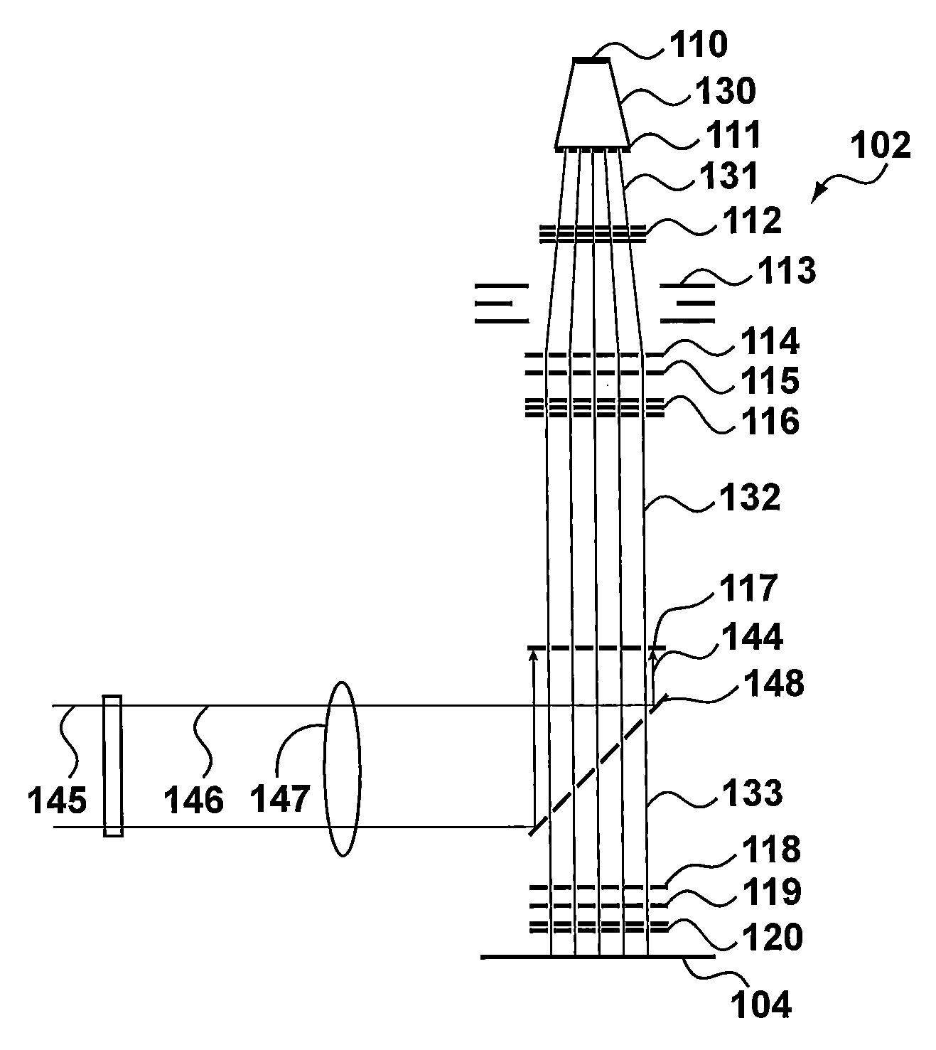
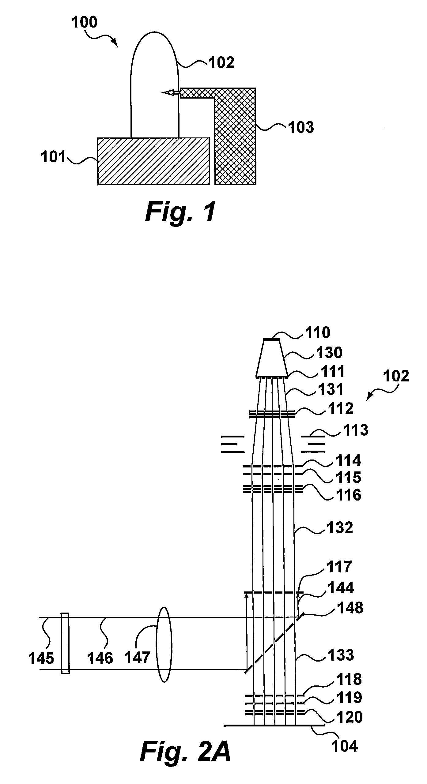
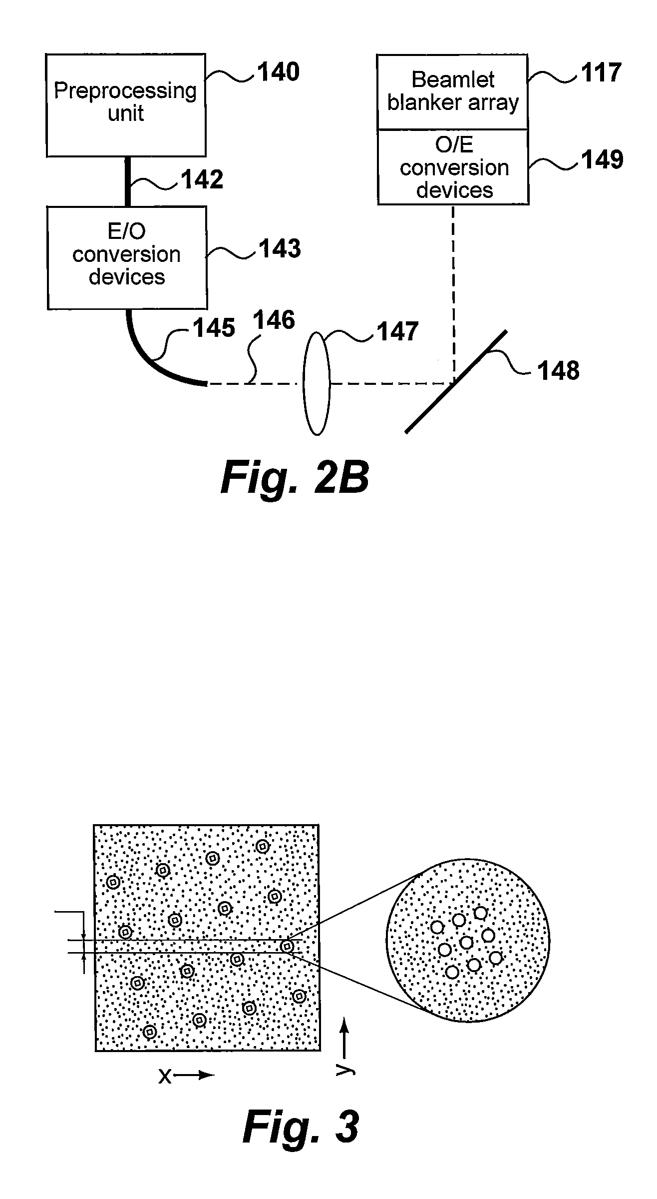
[0178]FIG. 8 shows an example of how the scan lines fill the stripe. The writing strategy determines how the scan lines will be written using the pattern of holes for the beamlets on the beamlet blanker array. One advantage of the “parallel projection” writing strategy is its efficiency. One electron beam is used to make the beamlets. Its efficiency depends on the ratio of the total area of holes (beamlets output current) compared to the area of the group of holes (beam input current). For a relative small number of holes (49), the area of the beam (group of beamlets) must be small for an acceptable efficiency. For “parallel projection” the beam (group) size is smaller that th...

second embodiment

[0325]FIG. 61 shows a second embodiment using in-line rasterization. This is similar to the FIG. 60 embodiment except corrections for beam position calibration, field size adjustment, and / or field position adjustment are made on the vector tool input data. Because these corrections are made on vector data, both full pixel shifts and subpixel shifts in the X and Y direction can be made. These corrections are typically performed in software, and may be performed per wafer. After the corrections have been made, rasterization is performed to generate the PSS format data for input to the pattern streamer.

[0326]FIG. 44 shows inline rasterization functional units assigned to process steps. For this architecture the functional units 3 and 4 (rasterization) are executed inline. For this option input data for the lithography system will be a stripe pattern description in vector format. The rasterization will be done on demand (per wafer, per several wafers, per series of wafers). Changes in g...


PUM


Abstract

A method for exposing a wafer using a plurality of charged particle beamlets. The method comprises identifying non-functional beamlets among the beamlets, allocating a first subset of the beamlets for exposing a first portion of the wafer, the first subset excluding the identified non-functional beamlets, performing a first scan for exposing the first portion of the wafer using the first subset of the beamlets, allocating a second subset of the beamlets for exposing a second portion of the wafer, the second subset also excluding the identified non-functional beamlets, and performing a second scan for exposing the second portion of the wafer using the second subset of the beamlets, wherein the first and second portions of the wafer do not overlap and together comprise the complete area of the wafer to be exposed.

Description

CROSS REFERENCE TO RELATED APPLICATIONS[0001]This application is a continuation of PCT application number PCT / IB2010 / 052217 filed on 19 May 2010, which claims priority from U.S. provisional application No. 61 / 179,762 filed on 20 May 2009. Both applications are hereby incorporated by reference in their entireties.BACKGROUND OF THE INVENTION[0002]1. Field of the Invention[0003]The present invention relates to a maskless charged particle lithography apparatus, and in particular to a data path, a method for implementing corrections, and a scanning method for such apparatus.[0004]2. Description of the Related Art[0005]A design for an integrated circuit is typically represented in a computer-readable file. The GDS-II file format (GDS stands for Graphic Data Signal) is a database file format which is the lithography industry standard for data exchange of integrated circuit or IC layout artwork. For lithography machines which use masks, a GDS-II file is typically used to manufacture a mask ...

Claims


Application Information

Patent Timeline
IPC IPC(8): G21K5/10
CPCB82Y10/00B82Y40/00H01J37/3177G03F7/70475H01J2237/31725H01J37/3174H01J37/3002H01J37/3175H01J2237/31722H01J37/045H01J37/3026H01J2237/3175H01L21/0274G06T1/20G06T1/60H01J2237/31761H01J2237/31764H04N1/405
Inventor VAN DE PEUT, TEUNISWIELAND, MARCO JAN-JACO
Owner ASML NETHERLANDS BV
Why Eureka
Try Eureka