Display device and electronic device

a technology of electronic devices and display devices, applied in the direction of semiconductor devices, electrical devices, transistors, etc., can solve the problem of insufficient field-effect mobility of transistors, and achieve the effect of adequate charging and discharging of signal lines and high current supply capabilities

Active Publication Date: 2012-11-15
SEMICON ENERGY LAB CO LTD
View PDF4 Cites 24 Cited by
  • Summary
  • Abstract
  • Description
  • Claims
  • Application Information

AI Technical Summary

Benefits of technology

[0065]The above-described transistor including a highly purified oxide semiconductor in a channel formation region has a field-effect mobility of as high as 80 cm2/Vs or more or 120 cm2/Vs, so that the transistor can have a high current supply capability even when formed over

Problems solved by technology

However, in the case where the analog switch is placed over the same substrate as the pixel portion, if a transistor used as the analog switch

Method used


Image

  • Display device and electronic device
  • Display device and electronic device
  • Display device and electronic device

Examples


embodiment 1

[0089]This embodiment describes a configuration of a display device having a signal line driver circuit including switch circuit portions.

[0090]A structural example of a display device is described with reference to FIG. 7. The display device includes a pixel portion 701, a scan line driver circuit portion 702, and a signal line driver circuit portion 703 over a substrate 700.

[0091]Note that as the substrate 700, in addition to a glass substrate and a ceramic substrate, a plastic substrate or the like with heat resistance can be used.

[0092]In the pixel portion 701, a plurality of pixels is provided for intersection portions of scan lines and signal lines. Since the video signal is supplied to respective pixels 704 through the signal lines in the pixel portion 701, an image with desired grayscale is displayed. In addition, a pixel electrode which is connected to a transistor and a display element is provided for each pixel. A gate electrode of the transistor is connected to a scan li...

embodiment 2

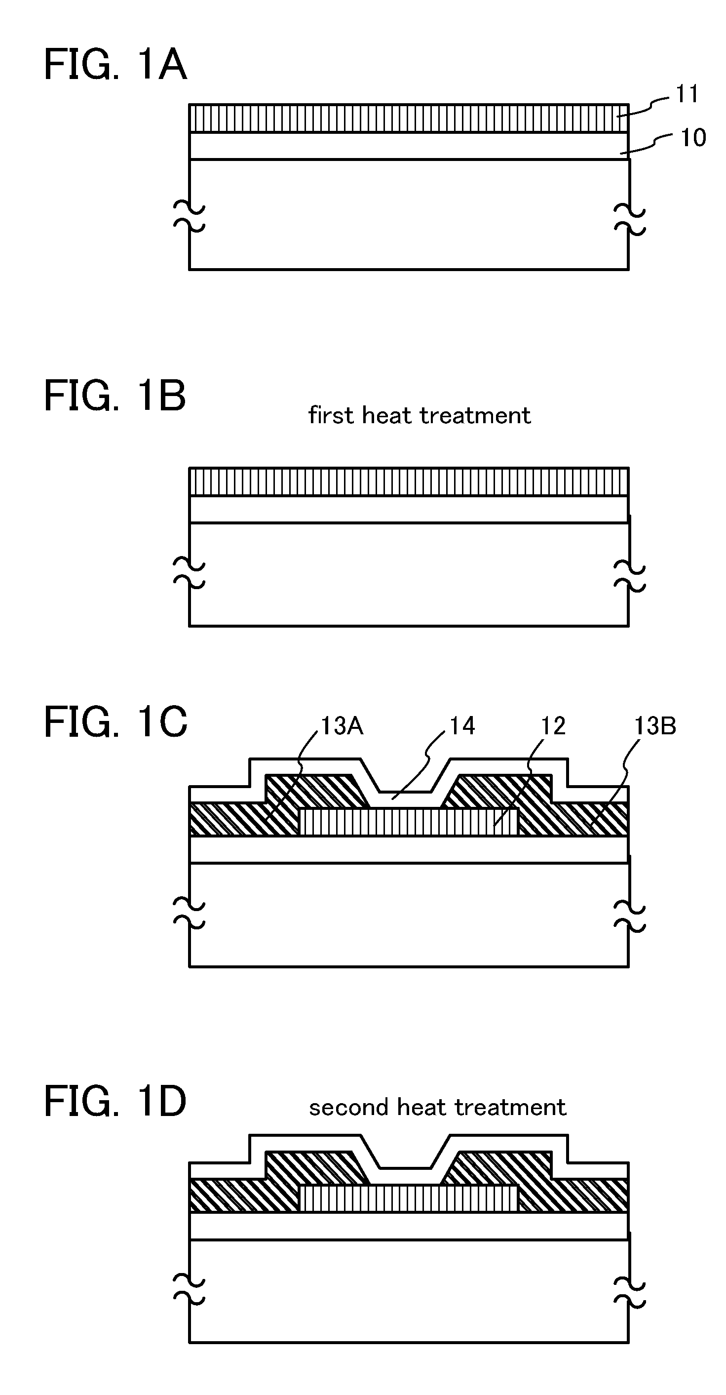
[0113]This embodiment describes an example of a method for manufacturing the transistors in the switch circuit portions described in Embodiment 1 with reference to FIGS. 11A to 11D and FIGS. 12A to 12D. FIGS. 13A and 13B and FIGS. 14A and 14B are examples of top views and cross-sectional views (taken along lines in the top views) of a transistor in each pixel in the pixel portion that can be formed over the same substrate as the transistors in the switch circuit portions.

[0114]This embodiment describes an example of a method for manufacturing a transistor with a bottom-gate structure, but the transistors in the switch circuit portions and the transistors in the pixels may have a top-gate structure. In addition, this embodiment describes an example of a method for manufacturing a staggered transistor, but a coplanar transistor can also be manufactured.

[0115]This embodiment describes an example of a method for manufacturing the transistors in the switch circuit portions, but the trans...

embodiment 3

[0177]In this embodiment, a c-axis aligned crystalline oxide semiconductor (CAAC-OS) film will be described.

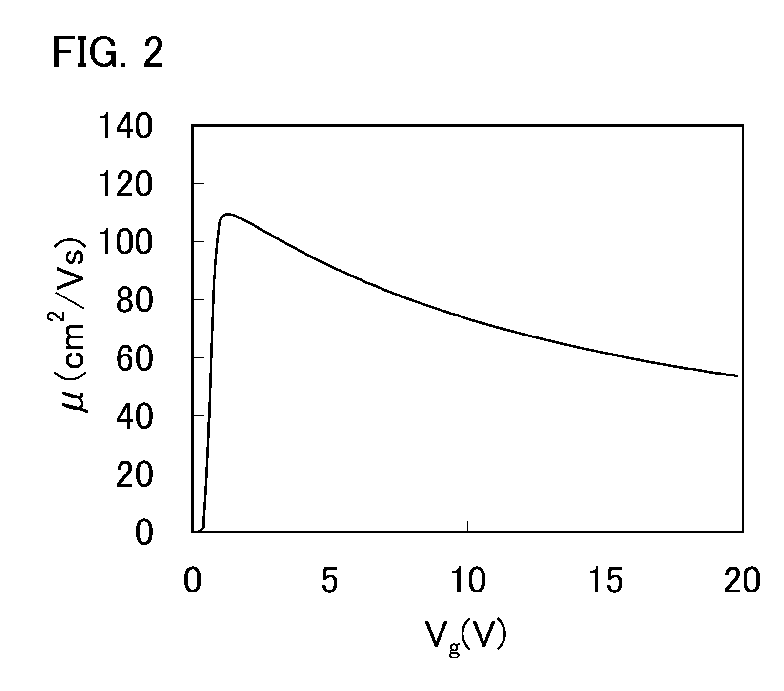
[0178]The CAAC-OS film is not completely single crystal nor completely amorphous. The CAAC-OS film is an oxide semiconductor film with a crystal-amorphous mixed phase structure where crystal parts and amorphous parts are included in an amorphous phase. Note that in most cases, the crystal part fits inside a cube whose one side is less than 100 nm. From an observation image obtained with a transmission electron microscope (TEM), a boundary between an amorphous part and a crystal part in the CAAC-OS film is not clear. Further, with the TEM, a grain boundary in the CAAC-OS film is not found. Thus, in the CAAC-OS film, a reduction in electron mobility, due to the grain boundary, is suppressed.

[0179]In each of the crystal parts included in the CAAC-OS film, a c-axis is aligned in a direction parallel to a normal vector of a surface where the CAAC-OS film is formed or a normal vecto...


PUM


Abstract

An object is, in a structure where switch circuits in a signal line driver circuit is placed over the same substrate as a pixel portion, to reduce the size of transistors in the switch circuits and to reduce load in the circuits during charging and discharging of signal lines due to the supply of data. A display device is provided which includes a pixel portion receiving a video signal, and a signal line driver circuit including a switch circuit portion configured to control output of the video signal to the pixel portion. The switch circuit portion includes a transistor over an insulating substrate. The transistor has a field-effect mobility of at least 80 cm2/Vs or more. The transistor includes an oxide semiconductor layer.

Description

BACKGROUND OF THE INVENTION[0001]1. Field of the Invention[0002]The present invention relates to a display device and an electronic device including the display device.[0003]2. Description of the Related Art[0004]With the widespread use of large display devices such as liquid crystal televisions, display devices are required to be higher-value-added and thus are under development. Particularly, a technique to form a driver circuit or part of a driver circuit over a substrate, where a pixel portion is formed, using thin film transistors (TFTs) whose channel region is formed using an amorphous semiconductor or a microcrystalline semiconductor is actively developed because the technique greatly helps a reduction in cost and improvement in reliability.[0005]Instead of forming a signal line driver circuit (a source driver) over a substrate where a pixel portion is formed, in a display device using transistors whose channel regions are formed using an amorphous semiconductor or a microcry...

Claims


Application Information

Patent Timeline
IPC IPC(8): H01L29/786
CPCH01L29/7869H01L27/1225H01L27/1244H01L27/127H01L29/24H01L29/78696
Inventor KOYAMA, JUNTANABE, TORU
Owner SEMICON ENERGY LAB CO LTD
Why Eureka
Try Eureka