Fin field-effect transistor and method for manufacturing the same

a field-effect transistor and transistor technology, applied in the field of semiconductor manufacturing technology, can solve the problems of affecting the affecting the electrical performance of the device, and affecting the accuracy of so as to solve the problem of inaccurate improve the accuracy of alignment, and facilitate the alignment of the contact plug

Active Publication Date: 2012-11-15
INST OF MICROELECTRONICS CHINESE ACAD OF SCI
View PDF6 Cites 24 Cited by
  • Summary
  • Abstract
  • Description
  • Claims
  • Application Information

AI Technical Summary

Benefits of technology

[0036]In the Fin Field-Effect Transistor and the method for manufacturing the same according to the embodiments of the present invention, when a fin has been formed, a dummy gate across the fin and a spacer of the dummy gate are formed on the fin, then, by using the dummy gate and the spacer as a mask and the isolation provided by them, a gate and a source / drain region equal in height are formed inside and outside the spacer, respectively. The upper surface of the gate and the upper surface of the source / drain region are in the same plane, making the alignment of the contact plug easier; and the gate and the source / drain region are separated by the spacer, which can improve alignment accuracy, solve inaccurate alignment of the contact plug, and improve the AC performance of the device.

Problems solved by technology

Those effects that are negligible in a long-channel model of MOSFET have become more significant, and in some cases, a major factor affecting the performance of the device.
The short-channel effect may degrade electrical performance of the device, causing problems such as decreased threshold voltage of the gate, increased power consumption and reduced signal-to-noise ratio.
For example, in one aspect, the channel of the device can be doped with more impurities such as phosphorus and boron, but this may cause carrier mobility decrease in the channel; in another aspect, stress in the channel can be enhanced, but strain increase is limited by the conventional SiGe Positive-channel Metal Oxide Semiconductor (PMOS) strained silicon technique; and in yet another aspect, the thickness of the gate oxide can be reduced, but we still face technological constraints: the reduction in thickness of the gate oxide does not match the reduction in width of the gate, resulting in increased the leakage current.
With the channel size continuing to shrink, the improvements can no longer resolve the increasingly significant short-channel effect.
However, the method above for forming a FinFET device has the problem that, in formation of the contact plug, the contact plug should be aligned with the gate, the source region and the drain region, and as the level of integration increases, the distance between gates is shortening, resulting in difficulty in the alignment of the contact plug and poor alignment accuracy.
Or, even if isolation between the contact plug at the source / drain region and the gate is realized, a large parasitic overlap capacitance will be formed therebetween, this may still reduce the AC performance and the speed of the device.

Method used


Image

  • Fin field-effect transistor and method for manufacturing the same
  • Fin field-effect transistor and method for manufacturing the same
  • Fin field-effect transistor and method for manufacturing the same

Examples


Embodiment Construction

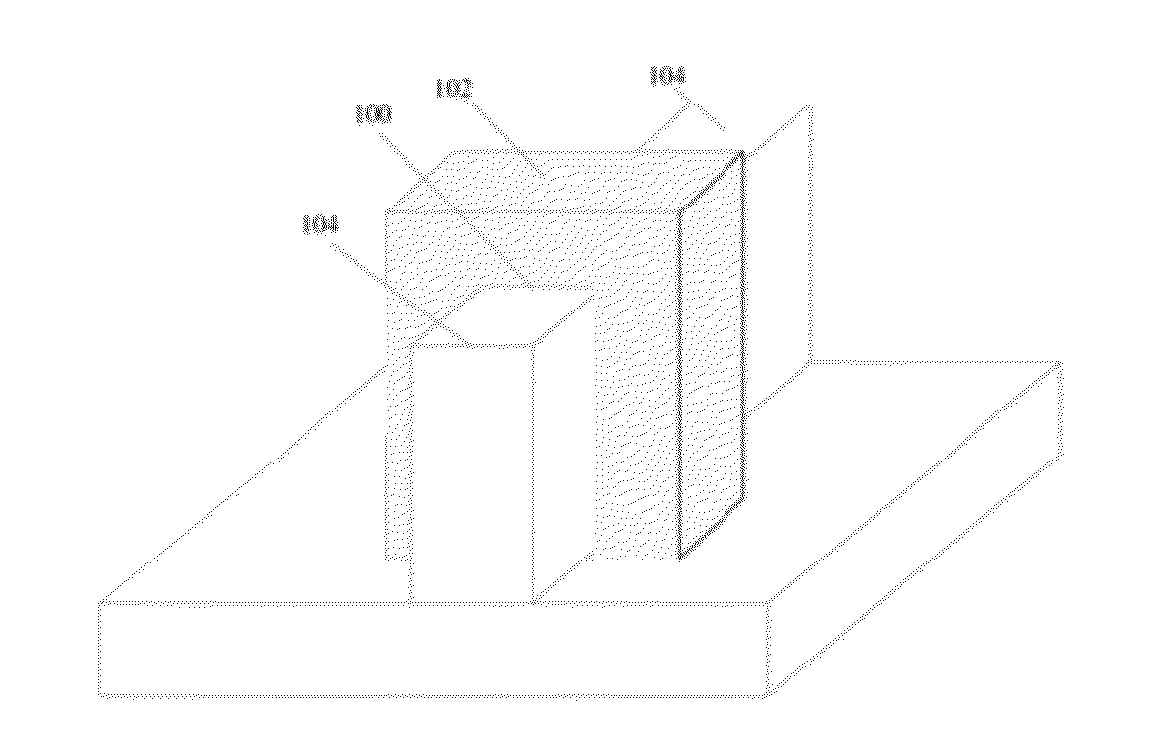
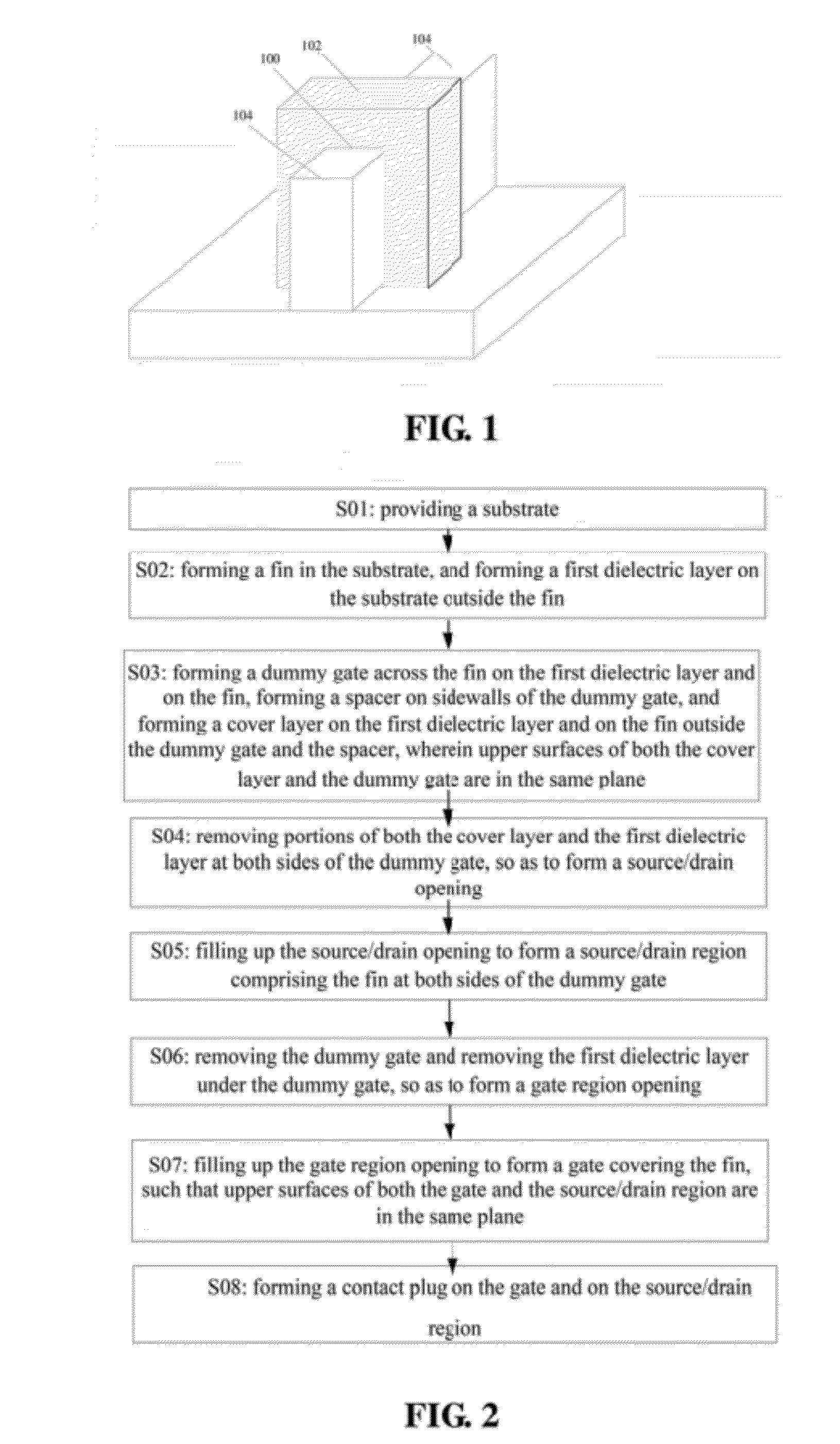
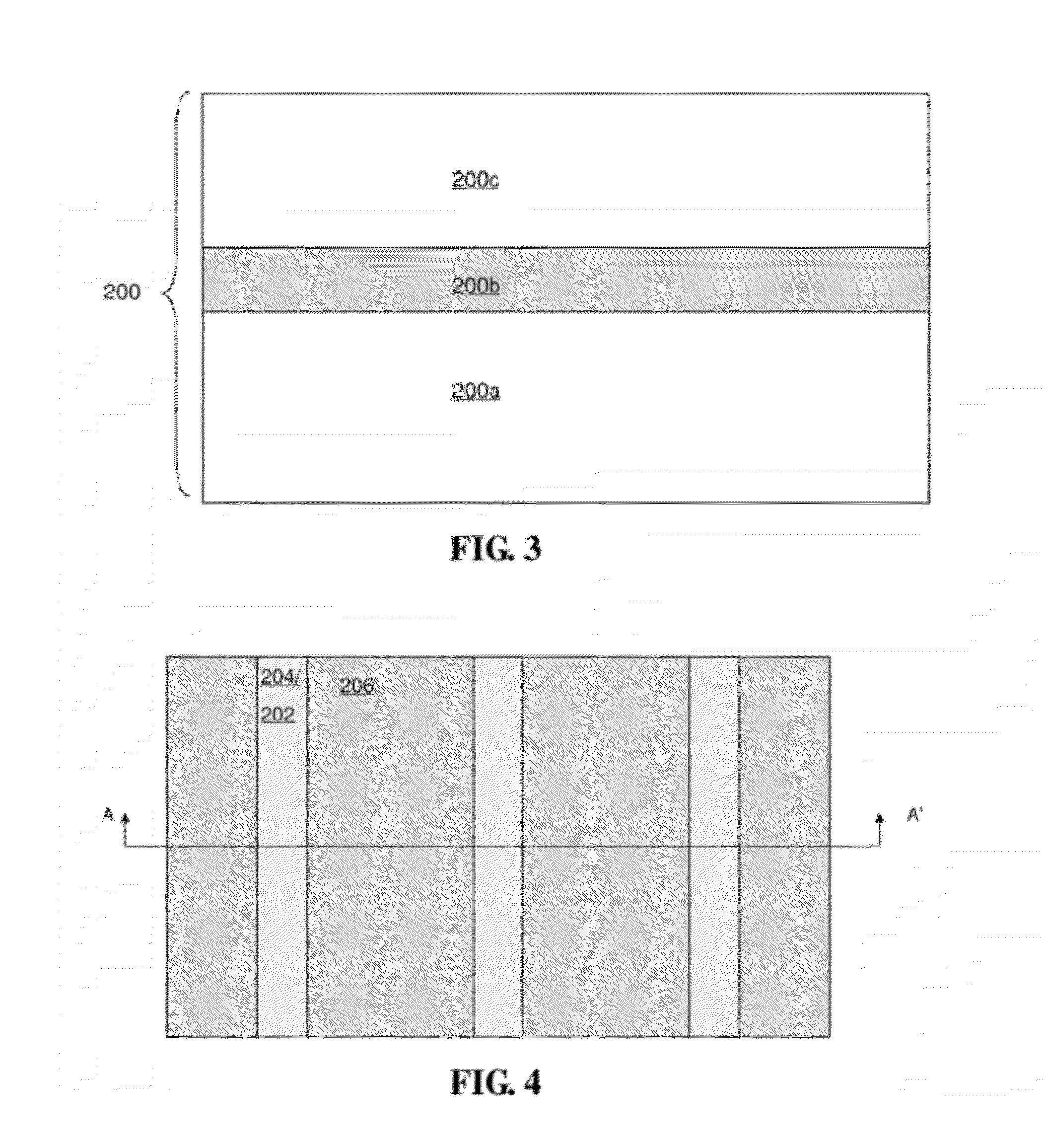
[0041]For a better understanding of the objects, features and advantages above of the present invention, the embodiments of the present invention will be described in details hereinafter with reference to the accompanying drawings.

[0042]In the following description, numerous specific details are set forth, in order to provide a thorough understanding of the present invention. It will be apparent to one skilled in the art that the present invention may be practiced without these specific details, and that equivalents to the present invention may be obtained without deviation from the essence of the present invention. Hence the present invention is not limited to the embodiments disclosed herein.

[0043]Moreover, the present invention is described in details in conjunction with the accompanying drawings. For illustrative purposes, the cross-sectional views of the device structures are locally and disproportionally enlarged, and do not limit the scope of protection of the present inventi...


PUM


Abstract

Embodiments of the present invention disclose a method for manufacturing a Fin Field-Effect Transistor. When a fin is formed, a dummy gate across the fin is formed on the fin, a spacer is formed on sidewalls of the dummy gate, and a cover layer is formed on the first dielectric layer and on the fin outside the dummy gate and the spacer, then, an self-aligned and elevated source/drain region is formed at both sides of the dummy gate by the spacer, wherein the upper surfaces of the gate and the source/drain region are in the same plane. The upper surfaces of the gate and the source/drain region are in the same plane, making alignment of the contact plug easier; and the gate and the source/drain region are separated by the spacer, thereby improving alignment accuracy, solving inaccurate alignment of the contact plug, and improving device AC performance.

Description

[0001]This application is a national phase application of, and claims priority to, PCT Application No. PCT / CN2011 / 078207, filed on Aug. 10, 2011, entitled “FIN FIELD-EFFECT TRANSISTOR AND METHOD FOR MANUFACTURING THE SAME,” which claimed priority to Chinese Application 201110116545.5, filed on May 6, 2011. Both the PCT application and Chinese application are incorporated herein by reference in their entireties.FIELD OF THE INVENTION[0002]The present invention relates to the field of semiconductor manufacturing technology, and more particularly to a Fin Field-Effect Transistor and a method for manufacturing the same.BACKGROUND OF THE INVENTION[0003]With the high level of integration in semiconductor devices, the channel length of a Metal-Oxide-Semiconductor Field-Effect Transistor (MOSFET) has become increasingly shorter. Those effects that are negligible in a long-channel model of MOSFET have become more significant, and in some cases, a major factor affecting the performance of the...

Claims


Application Information

Patent Timeline
Patent Type & Authority Applications(United States)
IPC IPC(8): H01L21/336H01L29/78
CPCH01L21/823431H01L21/845H01L29/66545H01L27/1211H01L27/0886
Inventor LIANG, QINGQINGZHONG, HUICAIZHU, HUILONG
Owner INST OF MICROELECTRONICS CHINESE ACAD OF SCI
Why Eureka
Try Eureka