

Word line divider and storage device
a word line divider and storage device technology, applied in the field of storage devices, can solve the problems of large circuits connected to sub-word lines affecting high integration, dram loss of data, unstable operation, etc., and achieve the effects of simplified circuit structure, stable operation, and simplified circuit structur
- Summary
- Abstract
- Description
- Claims
- Application Information
AI Technical Summary
Benefits of technology
Problems solved by technology
Method used
Image

Examples
embodiment 1
[0057]In this embodiment, structure examples of a word line divider according to one embodiment of the present invention and a storage device including the word line divider are described with reference to FIG. 1, FIG. 2, and FIG. 3.
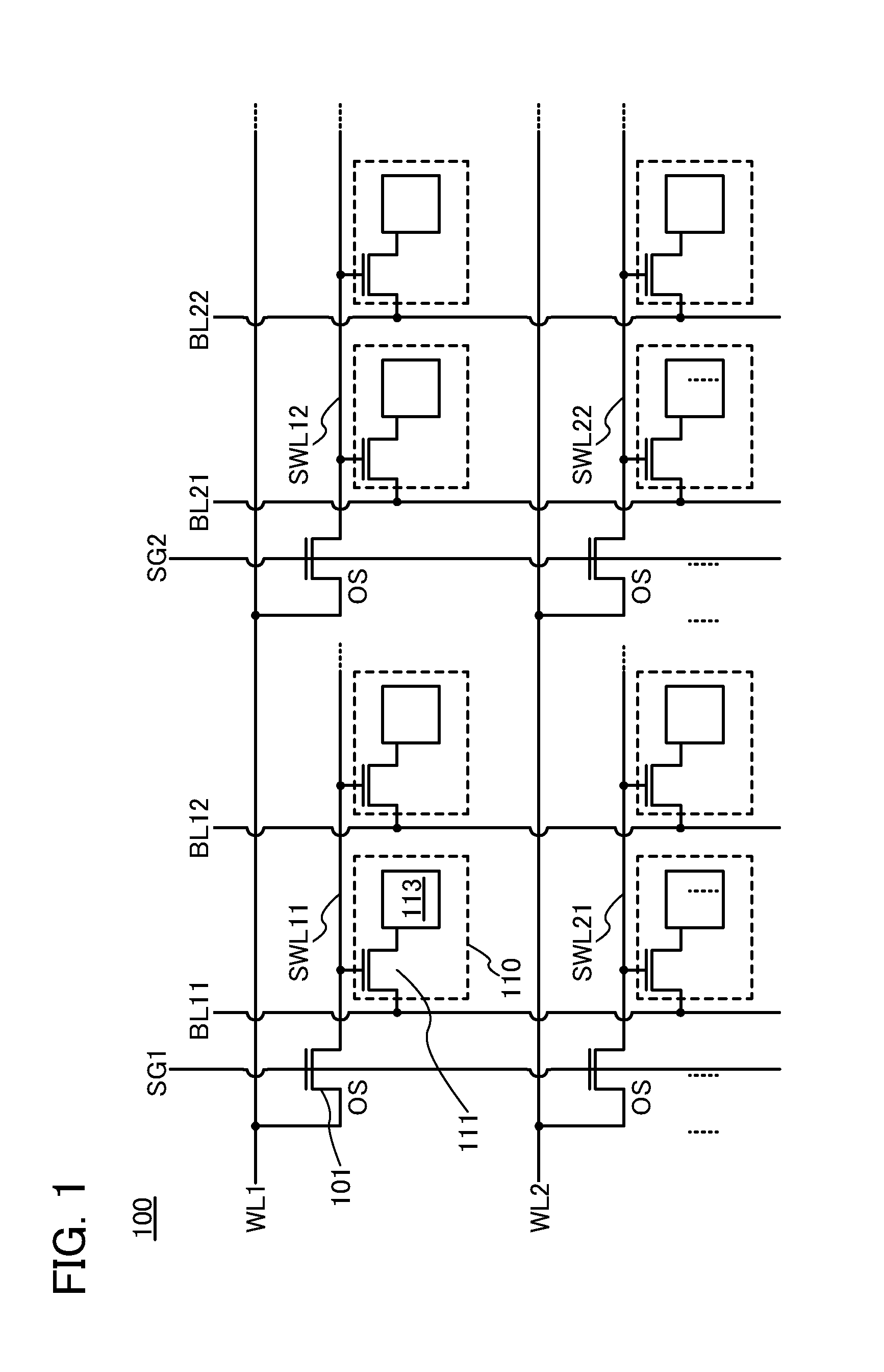
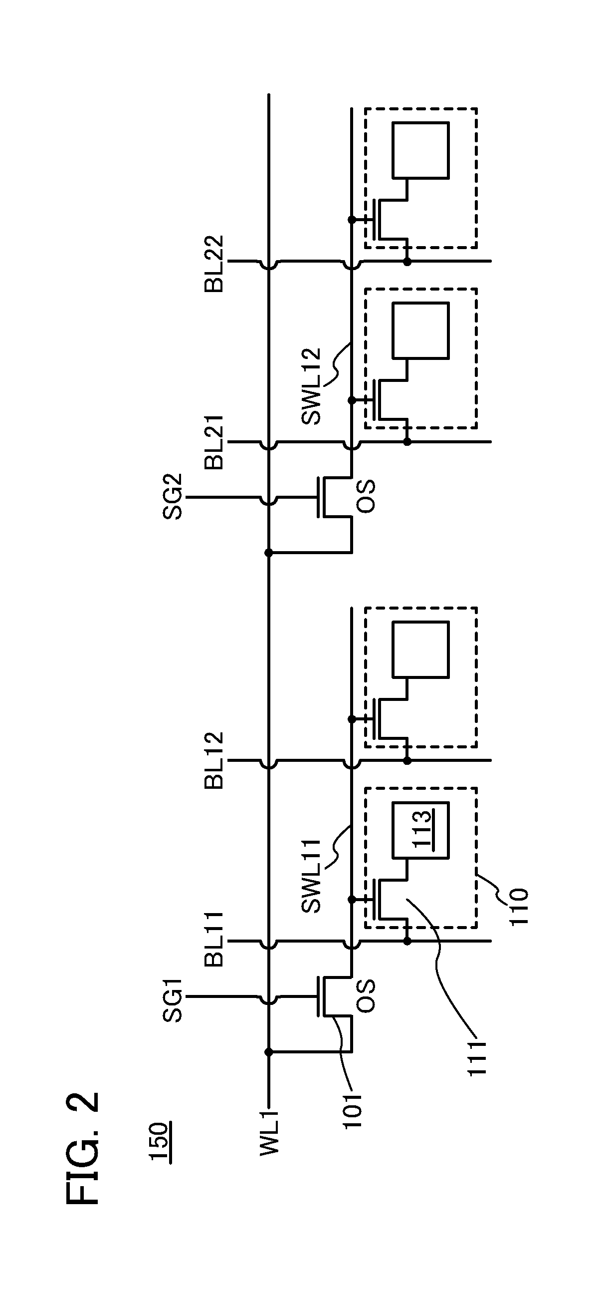
[0058]A storage device 100 illustrated in FIG. 1 includes a plurality of memory cells arranged in a matrix of m rows by (n×l) columns (m and l are each an integer of 1 or more and n is an integer of 2 or more). Note that for clarity, FIG. 1 illustrates a structure where m, n, and l are each 2.
[0059]The storage device 100 includes m word lines WLm, n selection signal lines SGn, (n×l) bit lines BLnl, (m×n) sub word lines SWLmn, and a plurality of memory cells 110 that are connected to the sub word lines SWLmn and the bit lines BLnl.
[0060]The memory cell 110 includes at least one selection transistor 111 and a data retention portion 113. A gate of the selection transistor 111 is connected to one of the sub word lines SWLmn. A first electrode of the selectio...
embodiment 2
[0086]In this embodiment, more specific structure examples of the storage device illustrated in Embodiment 1 are described with reference to FIG. 4, FIG. 5, FIG. 6, and FIG. 7.
[0087]Note that a description that overlaps with the description of the portions in Embodiment 1 is omitted or simply given.
structure example 1
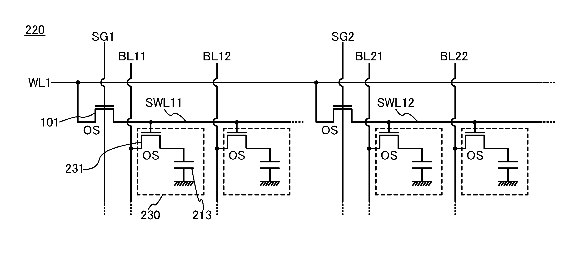
[0088]FIG. 4 is an example in which a DRAM memory cell is used as the memory cell 110 in the storage device 100 illustrated in Embodiment 1.
[0089]A storage device 200 illustrated in FIG. 4 includes a plurality of memory cells 210. Note that the structure of the storage device 200 is similar to the structure of the storage device 100 except for the memory cells.
[0090]The memory cell 210 includes a selection transistor 211 and a capacitor 213. A second electrode of the selection transistor 211 is connected to one electrode of the capacitor 213. A common potential is applied to the other electrode of the capacitor 213. In this structure example, the selection transistor 211 is an n-channel transistor. Here, instead of the common potential, a reference potential or a ground potential may be used. Further, a potential between two kinds of potentials input to a bit line is preferably used as the reference potential because voltage applied to the capacitor 213 can be reduced and dielectric...
PUM
 Abstract
Description
Claims
Application Information