Carbon nanotube dispersion liquid and method for manufacturing semiconductor device

Inactive Publication Date: 2012-11-22
NEC CORP
View PDF17 Cites 15 Cited by
  • Summary
  • Abstract
  • Description
  • Claims
  • Application Information

AI Technical Summary

Benefits of technology

[0025]According to the present invention, a stable dispersion liquid of CNTs can be obtained. In addition, the CNT dispersion liquid according to the present invention includes only components that can be removed by vaporization, other than CNTs. Therefore, a CNT random network formed using the CNT dispersion liquid according to the present invention is preferred for the current path of an electronic device, such as a thin film transistor, because substances that inhibit electrical conduction do not remain.
[0026]In addi

Problems solved by technology

A larger area is required of a display using such TFTs, but TFTs are usually fabricated on a glass substrate using amorphous or polycrystalline silicon and thus have the following problems in manufacture.
First, a CVD apparatus used for the manufacture of TFTs is very expensive, and its maintenance cost is also high, and the

Method used


Image

  • Carbon nanotube dispersion liquid and method for manufacturing semiconductor device
  • Carbon nanotube dispersion liquid and method for manufacturing semiconductor device
  • Carbon nanotube dispersion liquid and method for manufacturing semiconductor device

Examples


Example

First Exemplary Embodiment

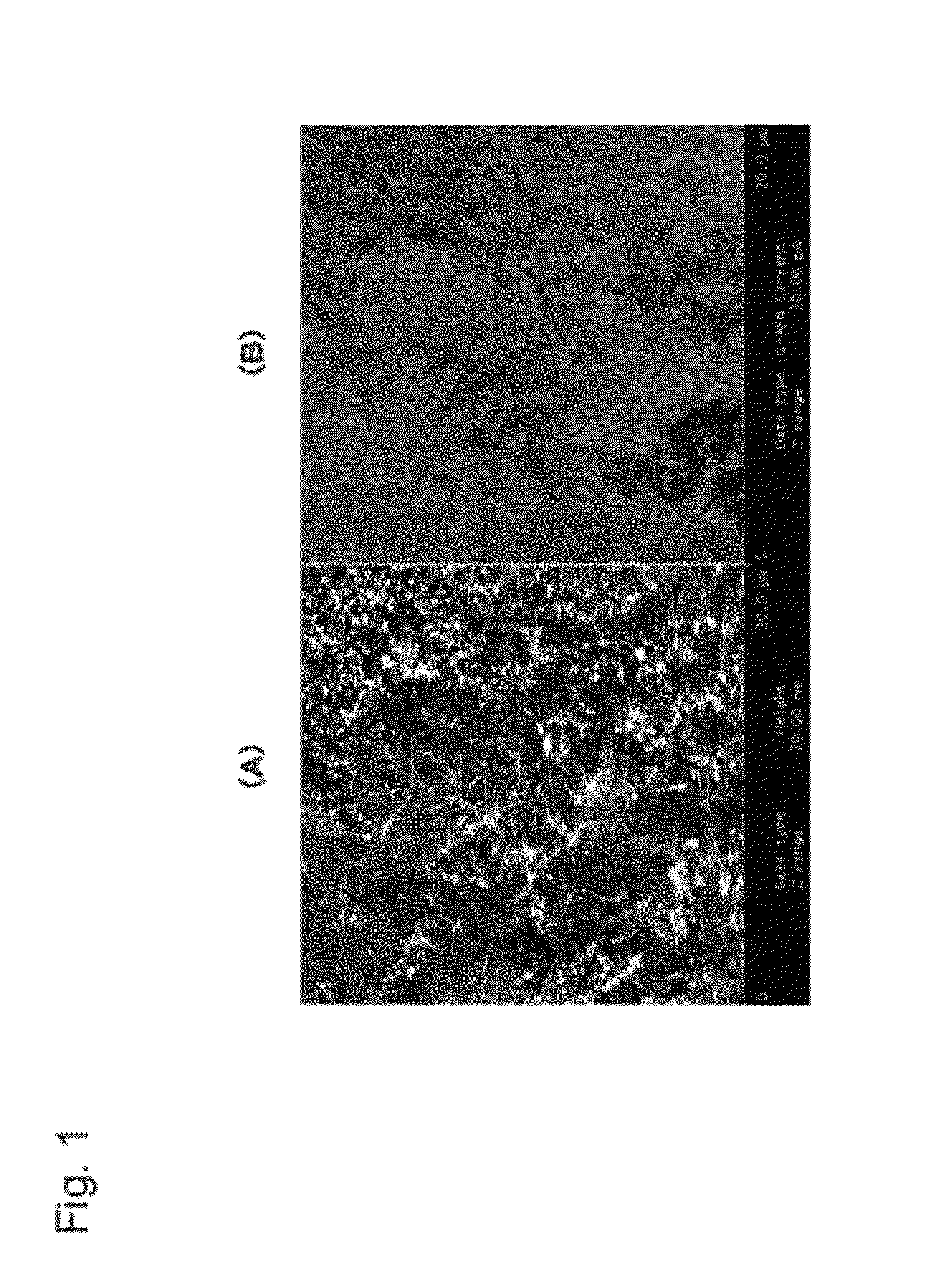
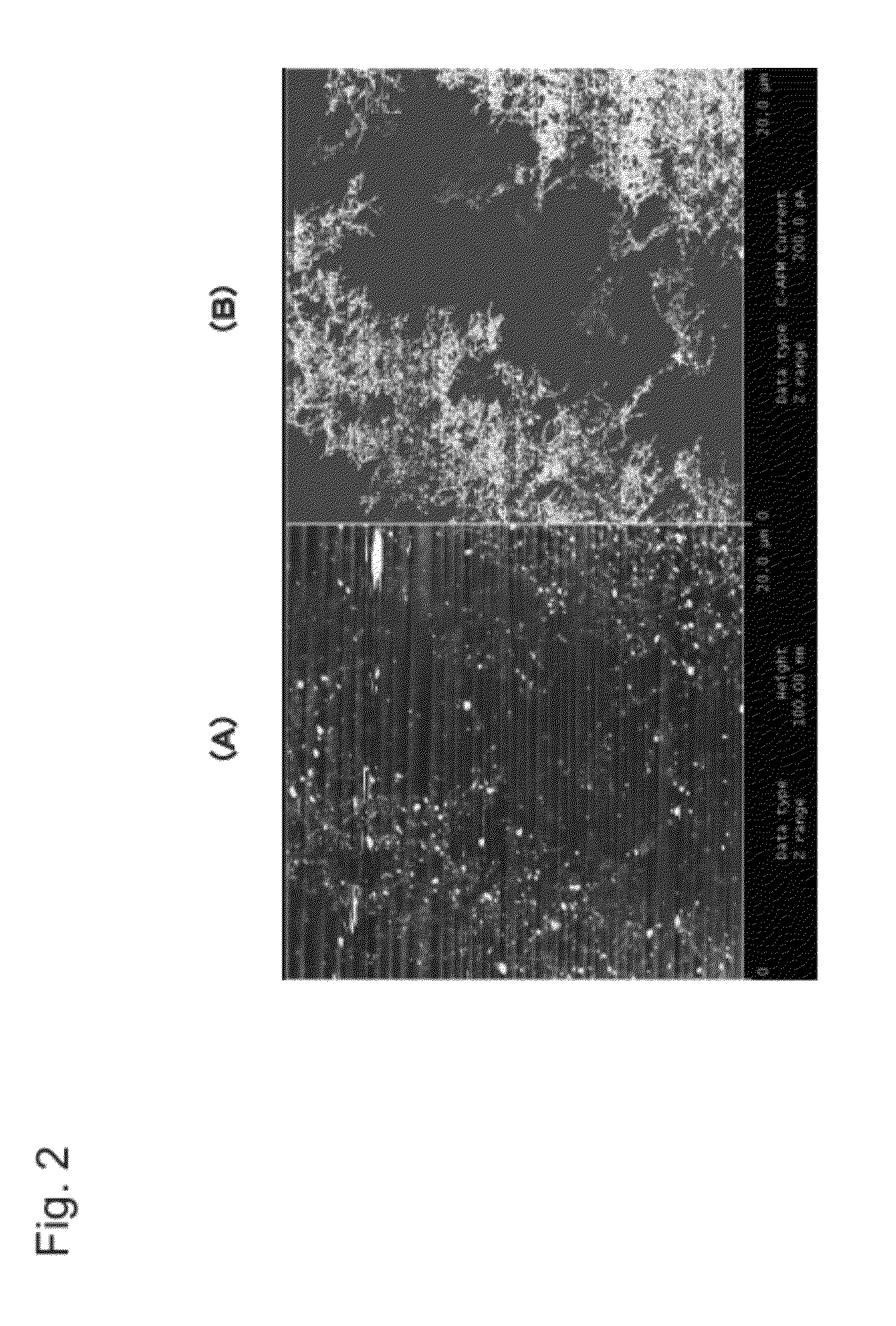
[0063]In this exemplary embodiment, single walled CNTs (SWCNTs) were added in the proportion of 1 mg to 100 ml of each of mixed solvents using xylene as a nonpolar first organic solvent and using various polar organic solvents as a second organic solvent, and the mixtures were further ultrasonically irradiated to prepare CNT dispersion liquids with a concentration of about 10 ppm.

[0064]The single walled CNTs used here were previously subjected to strong acid treatment, and a minute metal catalyst used during the synthesis of the CNTs, and amorphous carbon and the like produced simultaneously with the CNTs were removed, and the purity of the CNTs was increased. It is generally known that in such single walled CNTs whose purity is increased through strong acid treatment, the surface is provided with a functional group, such as a carboxyl group, contributing to dispersibility. For the single walled CNTs, those fabricated by the Hipco (High Pressure Carbon mono...

Example

Second Exemplary Embodiment

[0073]In this exemplary embodiment, single walled CNTs were added in the proportion of 1 mg to 100 ml of each of mixed solvents using n-tetradecane as a nonpolar first organic solvent and using various polar organic solvents as a second organic solvent, and the mixtures were further ultrasonically irradiated to prepare CNT dispersion liquids with a concentration of about 10 ppm.

[0074]For the single walled CNTs used here, single walled CNTs similar to those used in the first exemplary embodiment were used.

[0075]For the mixed solvents in this exemplary embodiment, n-tetradecane was used as the nonpolar first organic solvent, and 1,2-dichloroethane (dielectric constant: 10.3), triethylene glycol dimethyl ether, diethylene glycol diethyl ether, diethylene glycol dimethyl ether (dielectric constant: 5.97), and isopropyl alcohol (dielectric constant: 18.62) were used as the second solvent mixed with the first organic solvent. The mixing ratio (mass ratio) of n-t...

Example

Third Exemplary Embodiment

[0083]In this exemplary embodiment, single walled CNTs were added in the proportion of 1 mg to 100 ml of each of mixed solvents using 1,2-dichloroethane as a polar second organic solvent and using various nonpolar organic solvents as a first organic solvent, and the mixtures were further ultrasonically irradiated to prepare CNT dispersion liquids with a concentration of about 10 ppm.

[0084]For the single walled CNTs used here, single walled CNTs similar to those used in the first exemplary embodiment were used.

[0085]For the mixed solvents in this exemplary embodiment, 1,2-dichloroethane (dielectric constant: 10.3) was used as the polar second organic solvent, and n-tetradecane, mesitylene (dielectric constant: 2.279), and xylene (the dielectric constant of m-xylene: 2.374) were used as the first organic solvent. The mixing ratio (mass ratio) of the first organic solvent to 1,2-dichloroethane, the second organic solvent, was 1:1.

[0086]As comparative examples,...


PUM


Abstract

A carbon nanotube dispersion liquid obtained by mixing carbon nanotubes, a first organic solvent that is a nonpolar solvent, and a second organic solvent that has a polarity higher than that of this first organic solvent and is compatible with this first organic solvent.

Description

TECHNICAL FIELD[0001]The present invention relates to a carbon nanotube dispersion liquid and a method for manufacturing a semiconductor device.BACKGROUND ART[0002]Thin film transistors (TETs) are widely used as pixel switching elements for displays, such as liquid crystal displays and EL displays. In addition, in recent years, TFTs have often been used for driver circuits for a pixel array on the same substrate.[0003]A larger area is required of a display using such TFTs, but TFTs are usually fabricated on a glass substrate using amorphous or polycrystalline silicon and thus have the following problems in manufacture. First, a CVD apparatus used for the manufacture of TFTs is very expensive, and its maintenance cost is also high, and therefore, a larger area of a display involves a significant increase in manufacturing cost. Secondly, the process for forming a film of amorphous or polycrystalline silicon is performed at extremely high temperature, and therefore, usable substrate ma...

Claims


Application Information

Patent Timeline
IPC IPC(8): H01B1/24H01L21/336B82Y40/00B82Y99/00
CPCB82Y10/00B82Y30/00B82Y40/00C01B31/0273H01L51/0558H01L27/101H01L27/105H01L51/0007H01L51/0048C01B2202/02H01L29/0673C01B32/174H10K71/15H10K85/221H10K10/484
Inventor NUMATA, HIDEAKIENDOH, HIROYUKI
Owner NEC CORP
Why Eureka
Try Eureka