

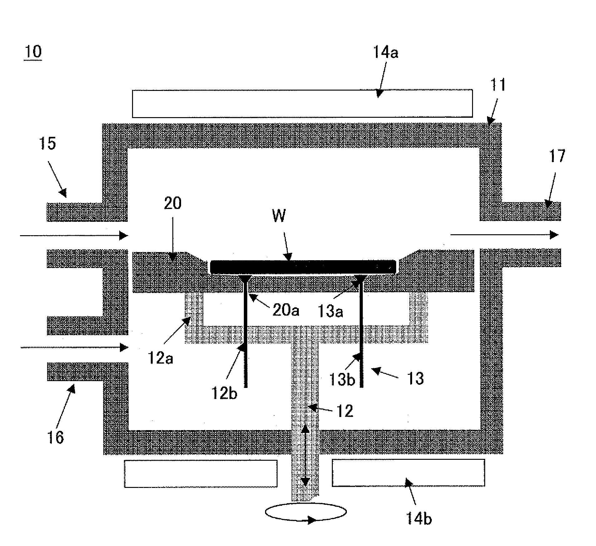
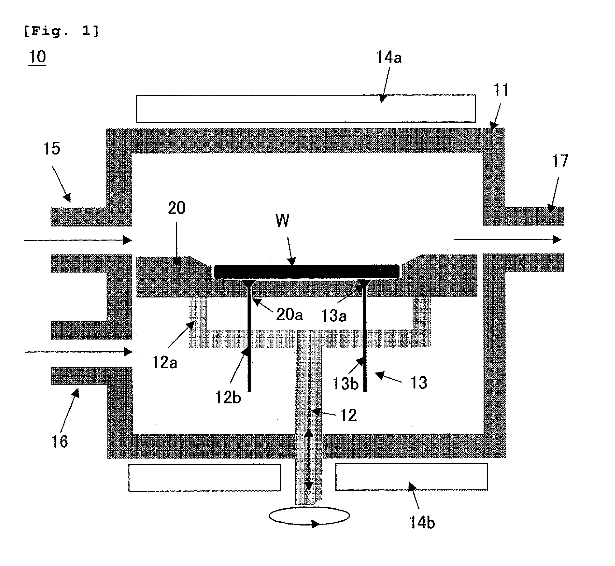
Vapor-phase growth semiconductor substrate support susceptor, epitaxial wafer manufacturing apparatus, and epitaxial wafer manufacturing method
a semiconductor substrate and support susceptor technology, applied in the direction of chemically reactive gases, crystal growth process, coatings, etc., can solve the problems of changing the thickness unable to selectively control the epitaxial layer thickness at the peripheral portion, etc., to achieve stably supplying the highly flat epitaxial wafer, easy control, and easy manufacturing of the epitaxial layer
- Summary
- Abstract
- Description
- Claims
- Application Information
AI Technical Summary
Benefits of technology
Problems solved by technology
Method used
Image

Examples
examples
[0099]Although the present invention will be more specifically explained hereinafter in conjunction with examples and comparative examples, the present invention is not restricted thereto.
examples 1 to 5
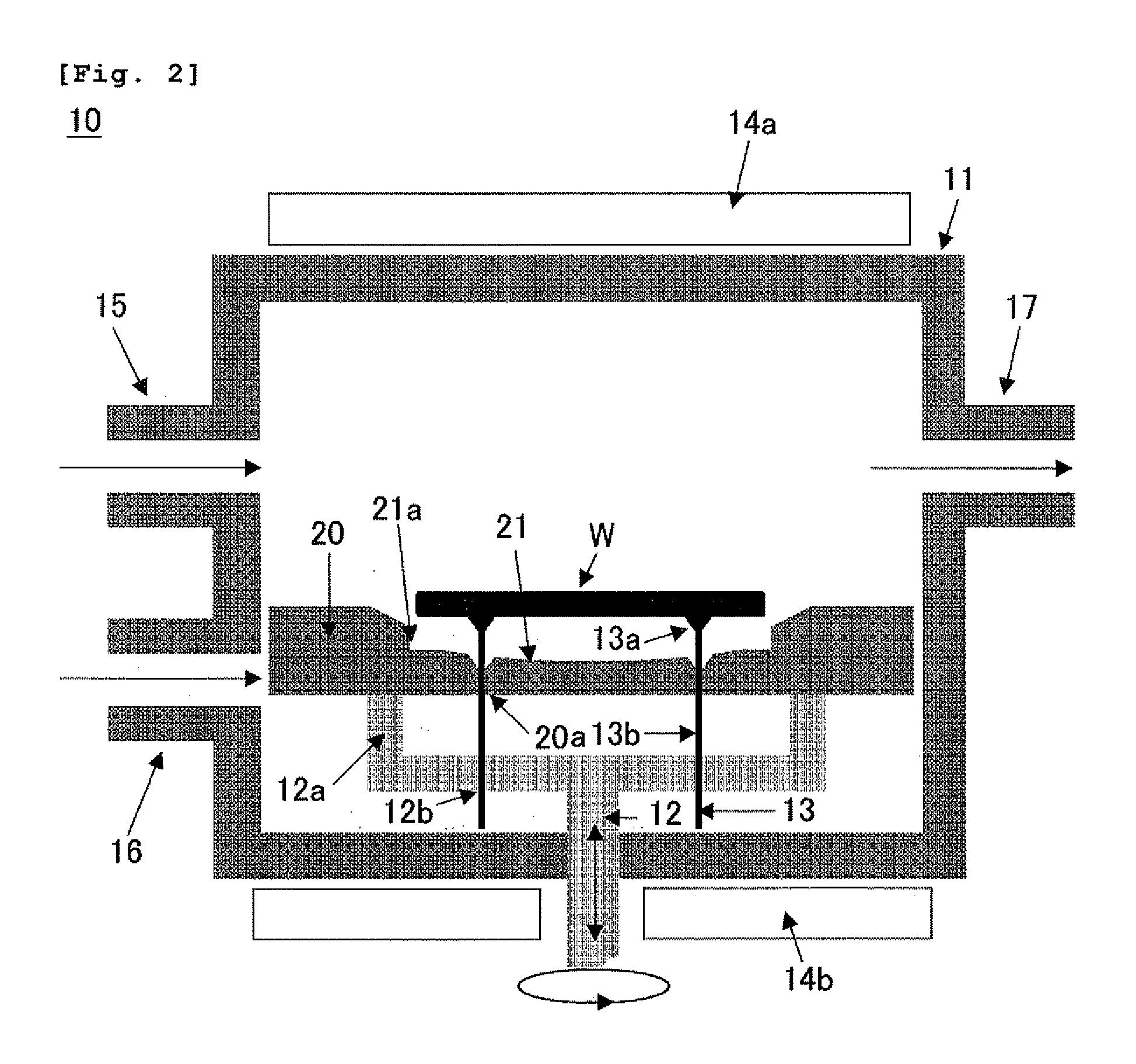
[0100]Such a susceptor as shown in FIG. 3 was fabricated. A pocket depth t of the susceptor was set to 800 μm close to a thickness of a silicon single crystal substrate, a height h of a taper was fixed to 100 μm, and a taper length (a length from a pocket edge to an outer side) d was set to d=22.5 mm in Example 1, d=15 mm in Example 2, d=10 mm in Example 3, d=7.5 mm in Example 4, and d=3 mm in Example 5 to fabricate five types of susceptors.
[0101]Table 1 collectively shows the parameters of each susceptor. It is to be noted that Table 1 and FIG. 7, which will be described later, show parameters of the susceptors according to later-described Comparative Examples 2 and 3 and variations in thicknesses of silicon epitaxial layers when these susceptors are used for comparison.
TABLE 1Ratio of taper length d toTaperTapersemiconductorPocketheightlengthsubstratedepth t [μm]h [μm]d [mm]diameter [%]Example 180010022.57.5Example 280010015.05.0Example 380010010.03.3Example 48001007.52.5Example 5...
examples 6 to 9
[0107]Such a susceptor as shown in FIG. 4 was fabricated. A pocket depth t of the susceptor was set to 800 μm close to a thickness of a silicon single crystal substrate, a height h of a taper was fixed to 100 μm, and a taper length (a length from a pocket edge to an outer side) d was set to d=22.5 mm in Example 6, d=15 mm in Example 7, d=7.5 mm in Example 8, and d=3 mm in Example 9 to fabricate four types of susceptors.
[0108]Table 2 collectively shows the parameters of each susceptor. It is to be noted that Table 2 and FIG. 8, which will be described later, show parameters of the susceptors according to later-described Comparative
[0109]Examples 1 and 2 and variations in thickness of silicon epitaxial layers when these susceptors are used for comparison.
TABLE 2Ratio of taper length d toTaperTapersemiconductorPocketheightlengthsubstratedepth t [μm]h [μm]d [mm]diameter [%]Example 680010022.57.5Example 780010015.05.0Example 88001007.52.5Example 98001003.01.0Comparative700———Example 1Com...
PUM
| Property | Measurement | Unit |
|---|---|---|
| flatness | aaaaa | aaaaa |
| flatness | aaaaa | aaaaa |
| flatness | aaaaa | aaaaa |
Abstract
Description
Claims
Application Information