Laser Resin Activation to Provide Selective Via Plating for Via Stub Elimination

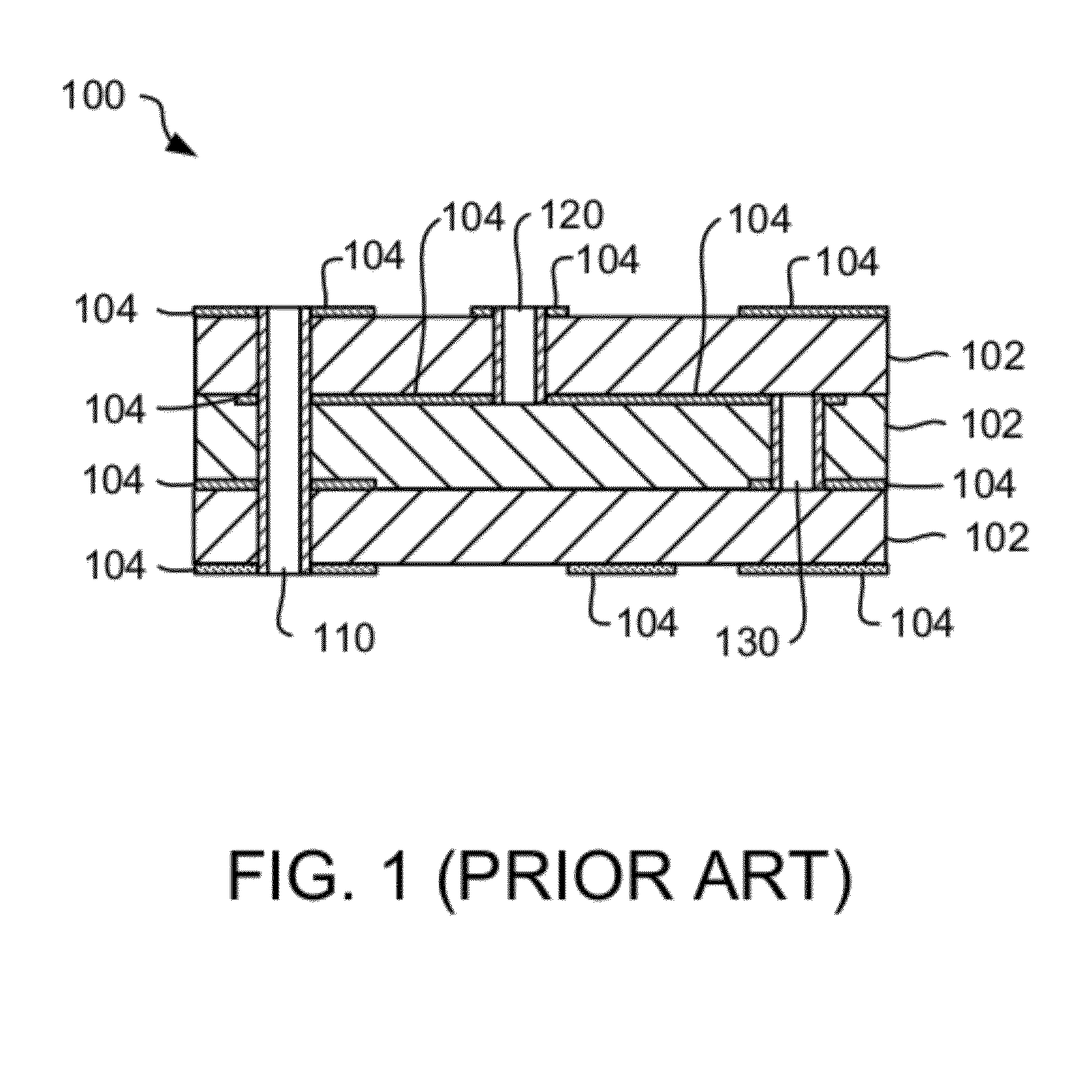
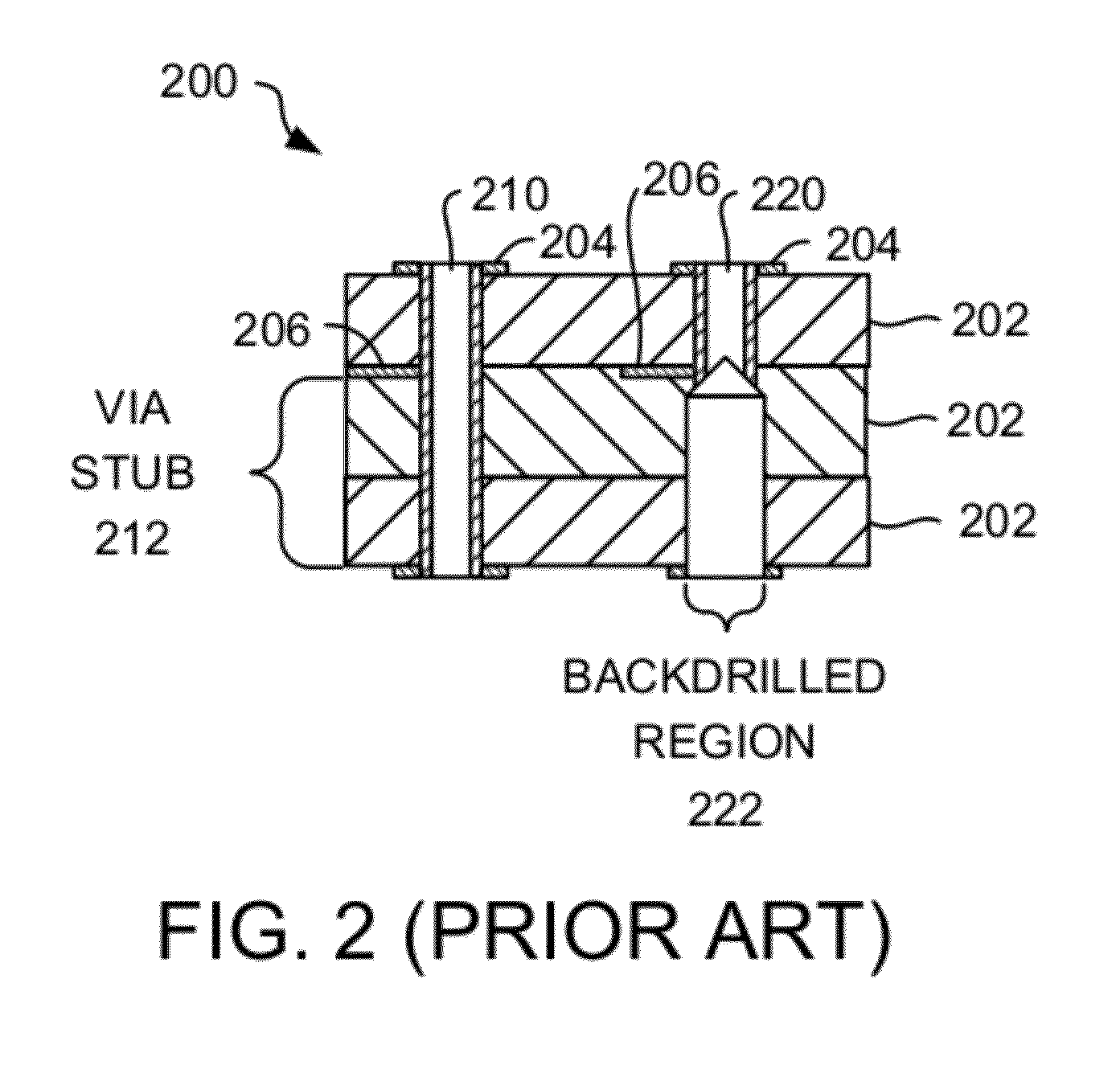
a technology of laser resin activation and selective via plating, which is applied in the field of selective via plating for eliminating via stubs, can solve the problems of buried vias, blind vias and buried vias are significantly more expensive to fabricate than pth vias, and backdrilling is a and achieve the effect of eliminating the costly and time-consuming process of backdrilling vias

Inactive Publication Date: 2012-12-13
IBM CORP
View PDF3 Cites 22 Cited by
  • Summary
  • Abstract
  • Description
  • Claims
  • Application Information

AI Technical Summary

Benefits of technology

[0009]According to the preferred embodiments of the present invention, laser resin activation is employed to provide selective via plating in printed wiring boards (PWBs) and other substrates. The selective via plating achieved by laser resin activation completely eliminates via stubs and the problems associated with via stubs. In one embodiment, the resin used in insulator layers of the PWB is formulated to contain spinel-based electrically non-conductive metal oxide. Preferably, only insulator layers through which vias will pass contain the metal oxide. Those layers are registered and laser irradiated at via formation locations to break do

Problems solved by technology

However, blind vias and buried vias are significantly more expensive to fabricate than PTH vias because blind vias and burie

Method used


Image

  • Laser Resin Activation to Provide Selective Via Plating for Via Stub Elimination
  • Laser Resin Activation to Provide Selective Via Plating for Via Stub Elimination
  • Laser Resin Activation to Provide Selective Via Plating for Via Stub Elimination

Examples


Embodiment Construction

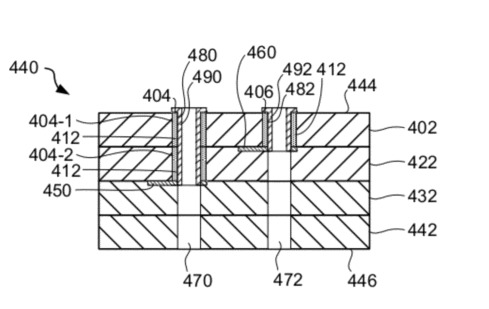
[0024]In accordance with the preferred embodiments of the present invention, laser resin activation is employed on a layer-by-layer basis to provide selective via plating and, thereby, achieve via stub elimination in printed wiring boards (PWBs) and other substrates, such as laminate subcomposites and interconnect substrates. To facilitate laser resin activation, at least one spinel-based electrically non-conductive metal oxide (e.g., the copper-containing spinel PK 3095 made by Ferro GmbH) is added to a conventional resin used to fabricate one or more insulator layers of the PWB. Preferably, only insulator layers through which vias will pass contain the metal oxide. Those layers are registered and laser irradiated at one or more via formation locations to break down the metal oxide and release metal nuclei. Laser irradiation is performed on a layer-by-layer basis to create areas of laminate that are electrically conductive and that can be dimensionally precisely controlled. This en...


PUM

PropertyMeasurementUnit
Electrical conductoraaaaaaaaaa

Abstract

An enhanced mechanism for via stub elimination in printed wiring boards (PWBs) and other substrates employs laser resin activation to provide selective via plating. In one embodiment, the resin used in insulator layers of the PWB contains spinel-based non-conductive metal oxide. Preferably, only insulator layers through which vias will pass contain the metal oxide. Those layers are registered and laser irradiated at via formation locations to break down the metal oxide and release metal nuclei. Once these layers are irradiated, all layers of the PWB or subcomposite are laid up and laminated. The resulting composite or subcomposite is subsequently drilled through and subjected to conventional PWB fabrication processes prior to electroless copper plating and subsequent copper electroplating. Because metal nuclei were released only in the via formation locations of the appropriate layers, plating occurs in the via barrels only along those layers and partially plated vias are created without stubs.

Description

BACKGROUND OF THE INVENTION[0001]1. Field of Invention[0002]The present invention relates in general to the electrical connector field. More particularly, the present invention relates to a method of eliminating a via stub in printed wiring boards (PWBs) and other substrates, such as laminate subcomposites and interconnect substrates. The present invention also relates to PWBs and other substrates fabricated using the method, and a design process therefor.[0003]2. Background Art[0004]Electrical connectors are in widespread use in the electronics industry. In many computer and other electronic circuit structures, an electronic module such as a central processor unit (CPU), memory module, application-specific integrated circuit (ASIC) or other integrated circuit, must be connected to a printed wiring board (PWB). Printed wiring boards are also known as printed circuit boards (PCBs). When populated with one or more electronic components, a printed wiring board is often referred to as a...

Claims


Application Information

Patent Timeline
IPC IPC(8): H05K1/00B32B38/04H05K3/46G06F17/50
CPCG06F17/5077H05K1/0251H05K3/429H05K3/4626Y10T156/1057H05K2203/107Y10T29/49155Y10T29/49165Y10T29/49126H05K2201/0209G06F30/394
Inventor BALCOME, GREGORY E.KRULL, BRETT P.KUCZYNSKI, JOSEPHRYKS, TERRY G.TOFIL, TIMOTHY J.
Owner IBM CORP
Why Eureka
Try Eureka