Optical semiconductor device, and manufacturing method thereof

a semiconductor and optical technology, applied in semiconductor lasers, cladded optical fibres, instruments, etc., can solve the problems of difficult control of mask shape or growth conditions, increased transition loss, stiff mode conversion from the upper core layer to the lower core layer, etc., to suppress propagation loss and improve conversion characteristics.

Active Publication Date: 2012-12-20
LUMENTUM JAPAN INC
View PDF0 Cites 39 Cited by
  • Summary
  • Abstract
  • Description
  • Claims
  • Application Information

AI Technical Summary

Benefits of technology

[0031]According to the invention, there are provided an optical semiconductor device which includes a spot-size converter improved in a c...

Problems solved by technology

In particular, in a manufacturing process of the thick film tapered spot-size converter, when the selective growth effect using a dielectric mask is used in crystal growth of the core layer 112, it is difficult to control the mask shape or...

Method used


Image

  • Optical semiconductor device, and manufacturing method thereof
  • Optical semiconductor device, and manufacturing method thereof
  • Optical semiconductor device, and manufacturing method thereof

Examples


first embodiment

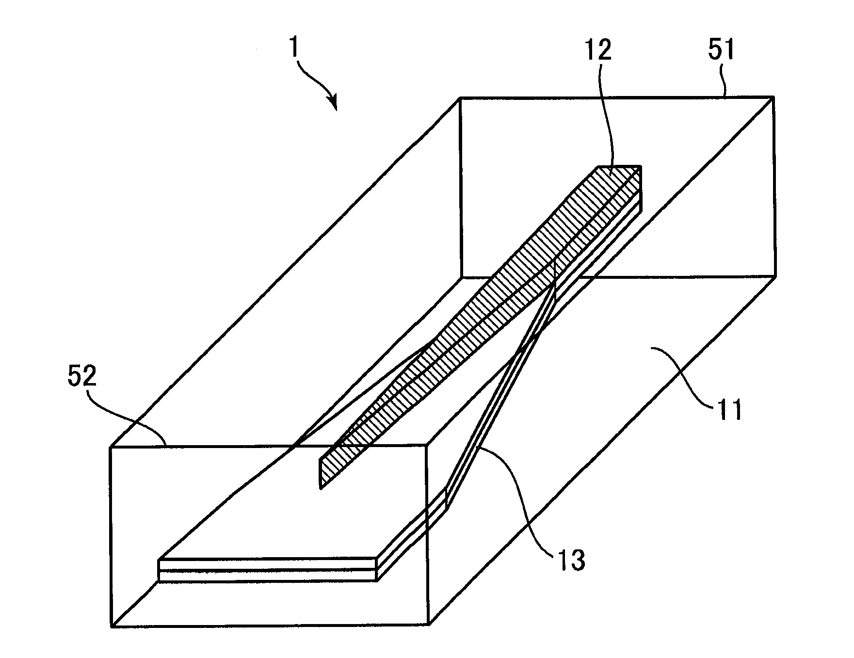
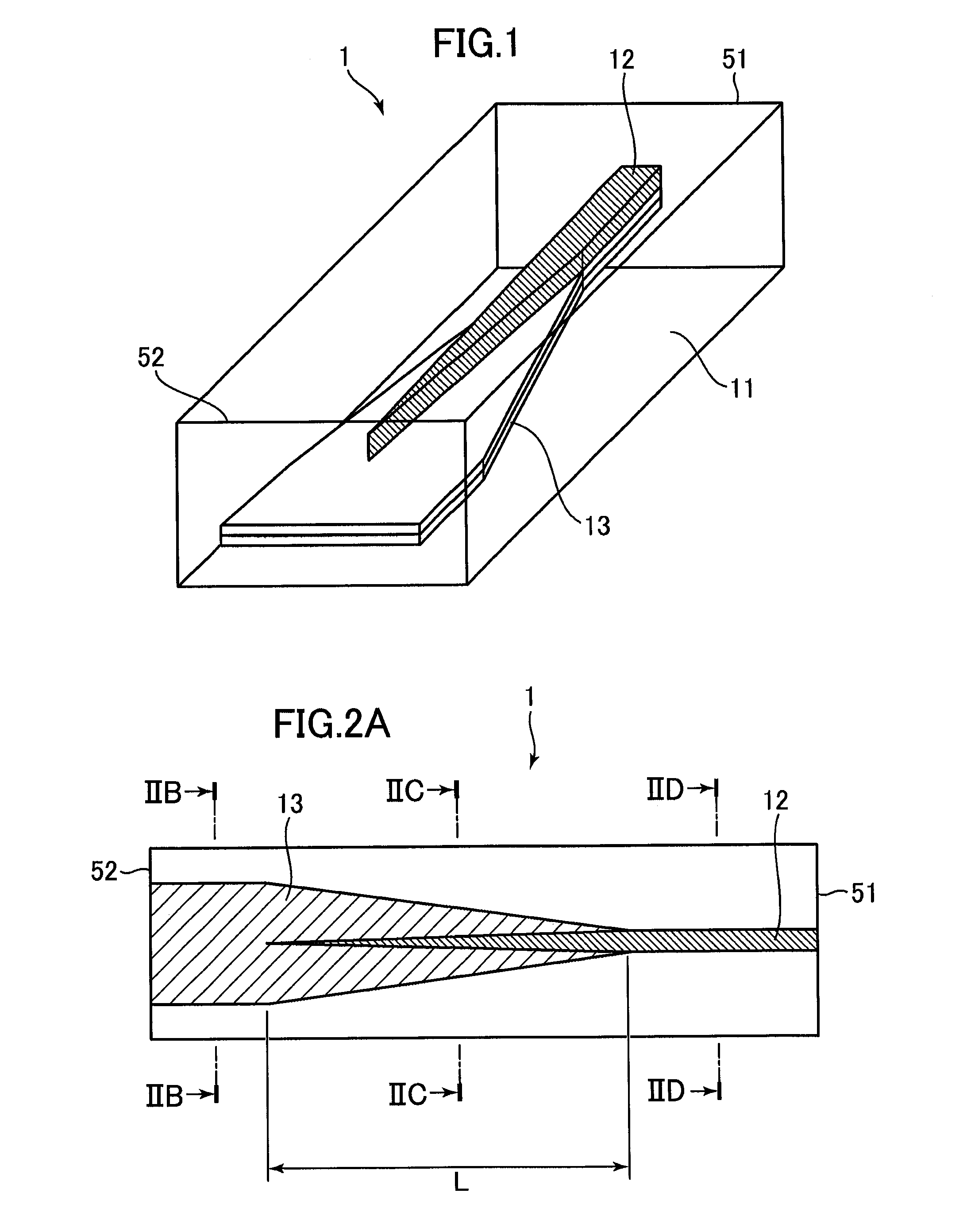
[0061]FIG. 1 is a schematic diagram illustrating a structure of a spot-size converter 1 according to a first embodiment of the invention. The spot-size converter 1 is a dual mesa tapered spot-size converter, as shown in FIG. 1. The spot-size converter 1 has a multilayer structure in which plural layers which includes an upper core layer 12 and a lower core layer 13 are layered. As described later in detail, the periphery of a two-layered core layer is surrounded by a clad layer 11. Further, in the spot-size converter 1, laser light is incident on the upper core layer 12 from a rear surface side in the figure, and the light propagated in the upper core layer 12 transits to the lower core layer 13. The spot-size converter 1 emits the laser light of which the spot size is converted, from a front surface side in the figure. That is, the rear surface shown in FIG. 1 corresponds to an incident end surface 51 and the front surface corresponds to an emission end surface 52. In a light trans...

second embodiment

[0082]An optical semiconductor device according to a second embodiment of the invention is an integrated semiconductor laser device 2 in which a spot-size converter section 3 and a gain section 4 of semiconductor laser are integrated on the same semiconductor substrate. Here, the semiconductor laser is a Fabry-Perot type laser having a band of 1.55 μm, and an InGaAsP-based material is used for a multiple quantum well layer 32.

[0083]FIG. 3A is a schematic top view illustrating a structure of the integrated semiconductor laser device 2 according to the second embodiment of the invention. FIG. 3A schematically shows a planar overlap in the spot-size converter 3 including the lower core layer 13 and the upper core layer 12 which is disposed above the lower core layer 13, when seen from the top of the integrated semiconductor laser device 2. Further, a p-type electrode 31 formed on an upper surface of the gain section 4 is shown, and an optical waveguide in the gain section 4 is schemati...

third embodiment

[0093]An optical semiconductor device according to a third embodiment of the invention is an integrated semiconductor laser device 5 in which the spot-size converter section 3 and a wavelength-variable laser section 6 are integrated on the same semiconductor substrate. The wavelength-variable laser section 6 is a wavelength-variable laser of an LGLC (Lateral Grating assisted Co-directional Coupler) type, and a structure of the wavelength-variable laser is disclosed in“Optical Fiber Communication Conference 2011, OWD7, March, 2011”.

[0094]FIG. 4A is a schematic top view illustrating a structure of the integrated semiconductor laser device 5 according to the third embodiment. As shown in FIG. 4A, a DBR section 7, a gain section 4 which generates light, a phase adjusting section 8 which adjusts the phase of light, and an LGLC filter section 9 are disposed in a wavelength-variable laser section 6 of an integrated semiconductor laser device 2, in the order from a light emission side. A fr...


PUM


Abstract

The optical semiconductor device includes a spot-size converter formed on a semiconductor substrate. The spot-size converter has a multilayer structure including a light transition region. The multilayer structure includes a lower core layer, and an upper core layer having a refractive index higher than that of the lower core layer. The width of the upper core layer is gradually decreased and the width of the lower core layer is gradually increased in the light transition region. Both sides and an upper side of the multilayer structure are buried by a semi-insulating semiconductor layer in the light transition region. Light incident from one end section of the spot-size converter is propagated to the upper core layer. The light transits from the upper core layer to the lower core layer in the light transition region, is propagated to the lower core layer, and exits from the other end section thereof.

Description

CROSS-REFERENCE TO RELATED APPLICATION[0001]The present application claims priority from Japanese application JP 2011-133575 filed on Jun. 15, 2011, the content of which is hereby incorporated by reference into this application.BACKGROUND OF THE INVENTION[0002]1. Field of the Invention[0003]The present invention relates to an optical semiconductor device, and a manufacturing method thereof.[0004]2. Description of the Related Art[0005]For example, an optical fiber is connected to a laser module having a semiconductor laser device. In this case, it is important to efficiently couple laser light emitted from the laser module to the optical fiber. With regard to an emission surface of a semiconductor laser device, in the case where optical confinement in an optical waveguide is strong, the far field pattern (hereinafter, referred to as FFP) of the laser light is widened, and a coupling efficiency with respect to the optical fiber is decreased. Further, in a case where the optical confin...

Claims


Application Information

Patent Timeline
IPC IPC(8): G02B6/036H01L21/02G02B6/12
CPCG02B6/305G02B6/1228G02B2006/12176H01S5/1014H01S5/026H01S5/06256H01S5/1032H01S5/2275H01S5/3054
Inventor SUZUKI, TAKANORITANIGUCHI, TAKAFUMI
Owner LUMENTUM JAPAN INC
Why Eureka
Try Eureka