Methods of Making Spatially Aligned Nanotubes and Nanotube Arrays

a technology of nanotubes and arrays, applied in the field of carbon nanotube materials, can solve the problems of limiting charge transport, limiting the mobilities of devices achieved with these networks, and the properties of transistors that use solution-deposited tubes are typically inferior to those of transistors, so as to achieve good electronic behavior (and/or optical properties), good placement accuracy, and high fidelity

Active Publication Date: 2012-12-20
THE BOARD OF TRUSTEES OF THE UNIV OF ILLINOIS
View PDF0 Cites 72 Cited by
  • Summary
  • Abstract
  • Description
  • Claims
  • Application Information

AI Technical Summary

Benefits of technology

[0049]The present invention also includes device arrays comprising spatially organized arrays of longitudinally aligned nanotubes in contact with one or more electrodes. Device arrays of the present invention may provide large area, electronic systems and / or mechanically flexible systems. An advantage of printable nanotube arrays of the present invention is that they may be fabricated in patterns on a mother substrate and subsequently patterned, for example using contact printing techniques, over large areas of a receiving substrate with good placement accuracy and high fidelity.
[0050]Guided growth and guided deposition methods of the present invention have their own benefits and limitations which make them suitable for a range of different device fabrication applications. For example, guided growth methods do not generally require exposure of longitudinally aligned nanotubes to surfactants, solvents, carrier liquids and / or other solution additives, which in some cases changes in the physical, optical and / or mechanical properties of the nanotubes. Guided deposition methods on the other hand, separate nanotube synthesis and alignment / orientation processing steps, therefore, allowing processing conditions for these steps to be independently selected, adjusted and / or optimized. Both guided deposition and growth methods are capable of generating highly dense arrays of longitudinally aligned nanotubes. This functional capability of guided growth methods of the present invention is beneficial for many device fabrication applications as the sheer number of and density of nanotubes in the array provides good electronic behavior (and / or optical properties) despite the existence of electronic (and / or optical) heterogeneity.

Problems solved by technology

The device mobilities that have been achieved with these networks are, however, still far below the intrinsic tube mobilities inferred from measurements of transistors that incorporate an individual tube (or small number of tubes) spanning the gap between the source and drain electrodes.
The resistance at the many tube—tube contacts that are inherent in the networks may limit charge transport.
Forming such arrays, patterning their coverage and, possibly, interfacing them with SWNT networks represent significant experimental challenges.
In addition, transistors that use solution-deposited tubes typically have properties that are inferior to those of transistors built with tubes grown directly on the device substrate by, for example, chemical vapor deposition (CVD).
However, high-density arrays that cover large areas have not been demonstrated with these techniques; device implementations have also not been described.

Method used


Image

  • Methods of Making Spatially Aligned Nanotubes and Nanotube Arrays
  • Methods of Making Spatially Aligned Nanotubes and Nanotube Arrays
  • Methods of Making Spatially Aligned Nanotubes and Nanotube Arrays

Examples


example 1

Spatially Selective Guided Growth of High Coverage Arrays of Single Walled Carbon Nanotubes and their Integration into Electronic Devices

[0122]Thin films of single-walled carbon nanotubes (SWNTs) can provide semiconducting and / or conducting components of passive and active (e.g. transistors) electronic devices. Potential applications range from large area, mechanically flexible systems, where semiconducting SWNT films could provide advantages over conventional small molecule or polymer semiconductors, to high performance devices, where they could provide alternatives to large grained polysilicon or even single crystal silicon. For the former class of application, random networks of SWNT might offer sufficient performance. For the latter, densely packed aligned arrays of SWNT are preferred. Forming such arrays, patterning their coverage and, possibly, interfacing them with SWNT networks represent significant experimental challenges. Modest degrees of alignment and coverage can be ach...

example 2

Guided Growth of Large-Scale, Horizontally Aligned Arrays of Single-Walled Carbon Nanotubes and their Use in Thin-Film Transistors

1. Introduction

[0135]In this example we describe use of large-scale arrays of longitudinally aligned carbon nanotubes as effective semiconductor “thin films” for TFTs. The effective device mobilities (up to 125 cm2V-1 s-1) are substantially higher than those that we have been able to achieve in random networks of SWNTs grown using similar techniques (≈50 cm2V-1 s-1). The results presented here indicate that low-cost quartz substrates can be used to generate high-quality aligned arrays of SWNTs for a range of applications in electronics and sensing.

2. Results and Discussion

[0136]FIG. 9 provides AFM images of random panel (a) and aligned panel (b) SWNTs grown on SiO2 and single-crystal quartz, respectively. Histograms are also presented in FIG. 9 of the orientation, panel (c), and diameter, panel (d), of the aligned SWNTs. These data suggest that most of th...

example 3

Transfer of Arrays of Longitudinally Aligned Nanotubes Grown on Guided Growth Substrates to Device Substrates

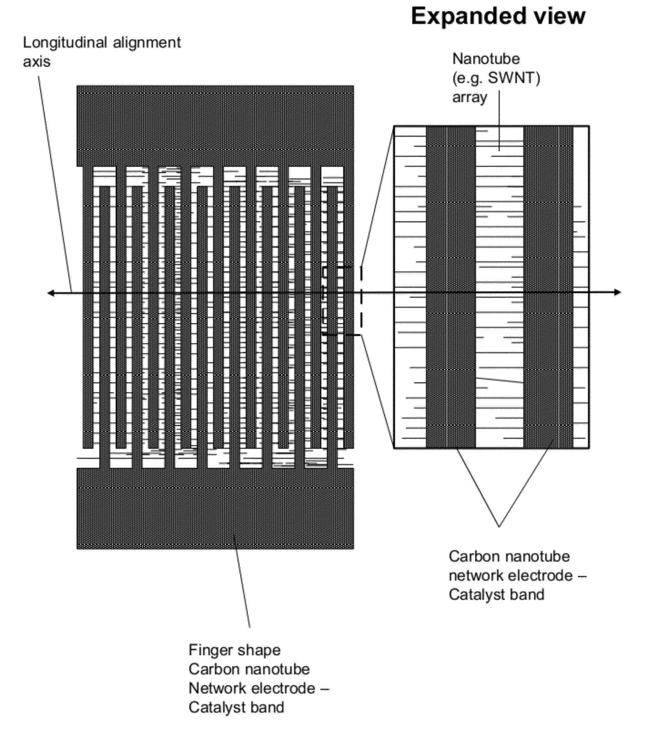
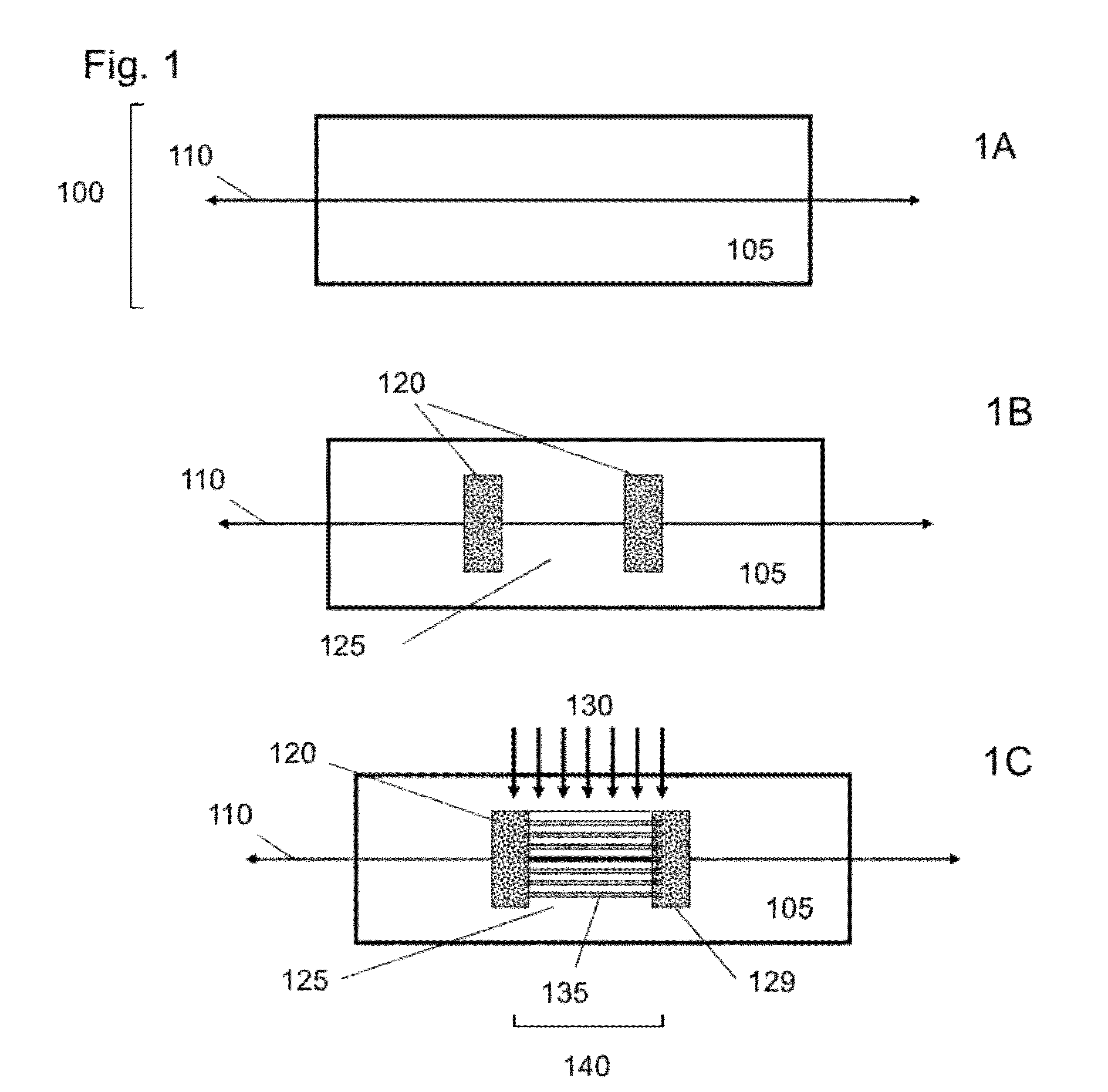
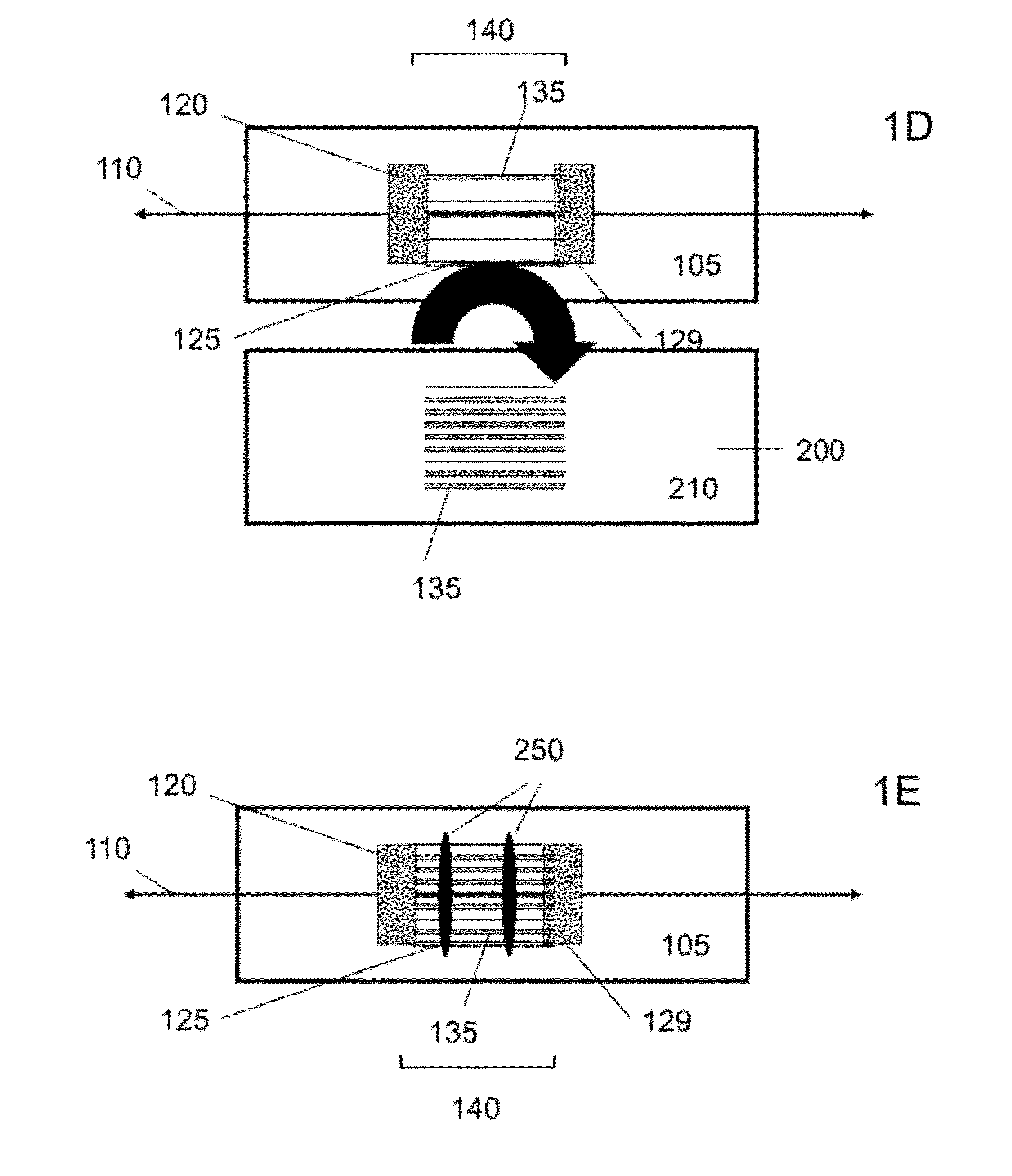
[0148]The present invention provides printable arrays of longitudinally aligned nanotubes fabricated on a guided growth substrate patterned with catalyst that are capable of subsequent transfer to a device substrate, such as a flexible polymer substrate or a substrate prepatterned with device components (e.g. electrodes, insulators, semiconductors etc.). Printable nanotube arrays of the present invention are capable of efficient transfer (e.g. at least 90% of the nanotubes are transferred) and are capable of transfer in a manner that preserves the relative orientations and positions of nanotubes in the array.

[0149]FIG. 17 shows a process flow diagram illustrating an exemplary method of the present invention for transferring one or more arrays of longitudinally aligned nanotubes from a guided grow substrate and assembling the transferred nanotubes into a functional device on a...


PUM

PropertyMeasurementUnit
cut angleaaaaaaaaaa
lengthaaaaaaaaaa
diametersaaaaaaaaaa

Abstract

The present invention provides arrays of longitudinally aligned carbon nanotubes having specified positions, nanotube densities and orientations, and corresponding methods of making nanotube arrays using guided growth and guided deposition methods. Also provided are electronic devices and device arrays comprising one or more arrays of longitudinally aligned carbon nanotubes including multilayer nanotube array structures and devices.

Description

CROSS-REFERENCE TO RELATED APPLICATIONS[0001]This application is a continuation of U.S. application Ser. No. 11 / 465,317, filed on Aug. 17, 2006 which claims priority under 35 U.S.C. 119(e) to U.S. provisional patent application 60 / 779,714 filed Mar. 3, 2006, each of which are hereby incorporated by reference in its entirety.STATEMENT REGARDING FEDERALLY SPONSORED RESEARCH OR DEVELOPMENT[0002]This invention was made with United States Government support under Contract Number 0403489 awarded by the National Science Foundation (NSF). The United States Government has certain rights in the invention.BACKGROUND OF INVENTION[0003]Since their discovery in the early 1990s, a great deal has been learned about the composition and properties of carbon nanotube materials. This research has demonstrated that carbon nanotubes exhibit extraordinary mechanical, electronic and chemical properties, which has stimulated substantial interest in developing applied technologies exploiting these properties...

Claims


Application Information

Patent Timeline
Patent Type & Authority Applications(United States)
IPC IPC(8): C23C16/26C23C16/56B82Y30/00B82Y40/00
CPCB82Y10/00B82Y30/00B82Y40/00C01B2202/02C01B2202/08C01B2202/34H01L51/0012H01L51/0048H01L51/0541H01L51/0545C01B32/162H10K71/191H10K85/221H10K10/464H10K10/466
Inventor ROGERS, JOHN A.KOCABAS, COSKUNSHIM, MOONSUBKANG, SEONG JUNPARK, JANG-UNG
Owner THE BOARD OF TRUSTEES OF THE UNIV OF ILLINOIS
Why Eureka
Try Eureka