Method and device for forming piezoelectric/pryoelectric film
- Summary
- Abstract
- Description
- Claims
- Application Information
AI Technical Summary
Benefits of technology
Problems solved by technology
Method used
Image
Examples
first embodiment
[0121]Now, the present invention will be explained.
[0122]PVDF (#850 manufactured by Kureha Corporation) and DMF (manufactured by Yamaichi Chemical Industries Co., Ltd.) are employed as a dielectric substance and a solvent, respectively. A dielectric solution is diluted at a mixing ratio of 4:96. An electric resistance value of the solution is 100 kΩ at this time. A material to be coated 18 is a copper plate with its length 100 mm, width 40 mm and thickness 0.8 mm (hereinafter referred to as the material to be coated 18).
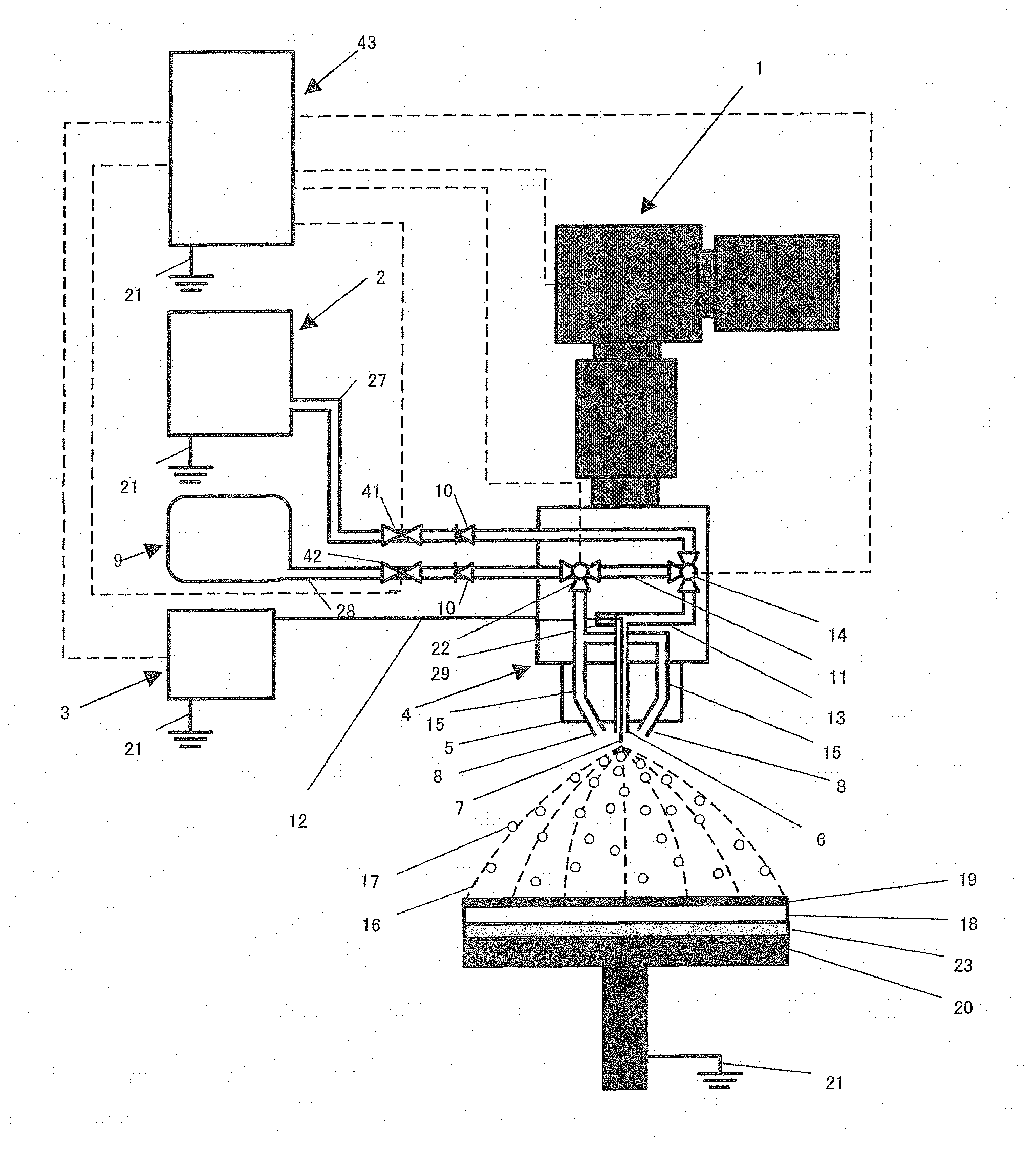
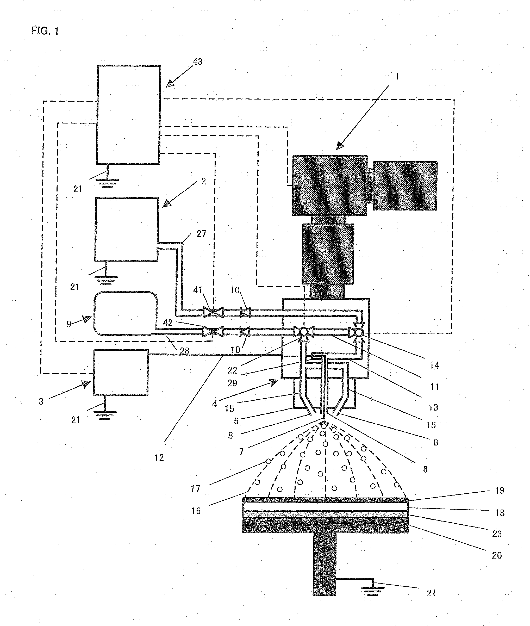
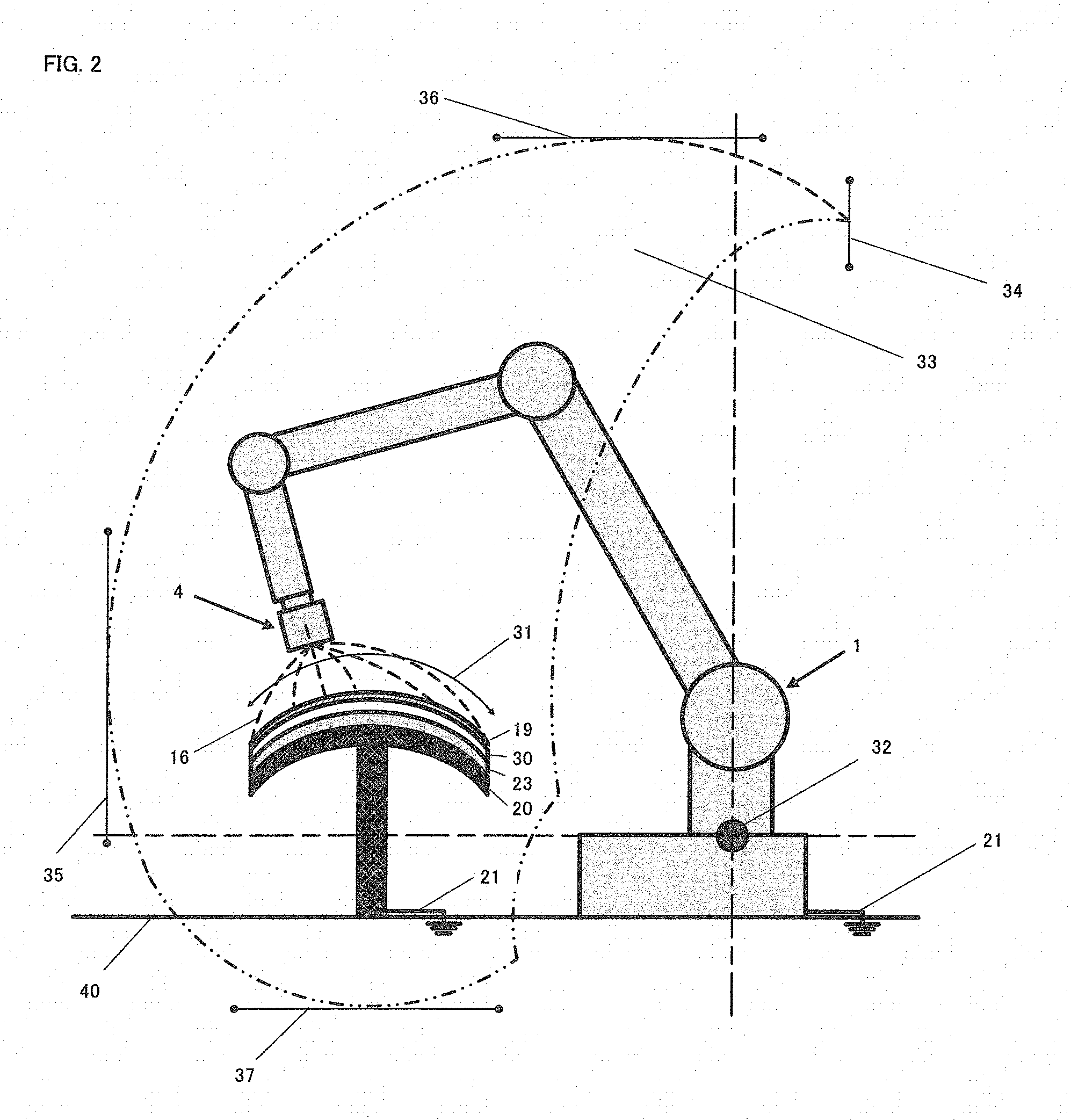
[0123]A coating sprayer 4 (manufactured by Munekata Co., Ltd.) is attached to a handling device 1, which is a handling robot (PX2850) manufactured by Yasukawa Electric Corporation. A center point of the coating sprayer 4 is aligned to a center point in width of the material to be coated 18. Then the coating sprayer 4 is moved along a longitudinal direction of the material to be coated 18.
[0124]An operable range corresponds to the length of the material to be coated 1...
PUM
| Property | Measurement | Unit |
|---|---|---|
| Temperature | aaaaa | aaaaa |
| Temperature | aaaaa | aaaaa |
| Electric potential / voltage | aaaaa | aaaaa |
Abstract
Description
Claims
Application Information


