Optoelectronic-Device Wafer Probe and Method Therefor

Inactive Publication Date: 2013-01-03
WALKER JAMES ALBERT
View PDF0 Cites 15 Cited by
  • Summary
  • Abstract
  • Description
  • Claims
  • Application Information

AI Technical Summary

Benefits of technology

[0013]The present invention enables improved coupling efficiency between optoelectronic devices (e.g., LEDs, VCSELs, super luminescent diodes, etc.) disposed on a wafer and one or more optical waveguides (e.g., optical fibers or PLC-based waveguides) located on a wafer probe head. As a result, the present invention enables wafer level testing of optoelectronic devices at a faster rate than can be attained with prior art systems and methods. Embodiments in accordance with the present invention enable the optica

Problems solved by technology

For optoelectronic devices, however, wafer-level testing is more complicated.
For optical sources, such as light emitting diodes (LEDs), vertical-cavity surface-emitting lasers (VCSELs), and the like, this can be very difficult as such devices typically emit light over a rather large range of angles.
The cost of LEDs (as compared to other illumination sources, such as incandescent bulbs, compact fluorescent bulbs, etc.), however, has thus far limited the widespread adoption of LEDs in cases.
Much of the cost associated with LEDs arises from the challenges inherent to wafer-level testing to determine its optical output power and spectral characteristics.
The time required for the analysis of the light is relatively short.
The time spent moving the probe head from device to device and settling it to enable a stable measurement can b

Method used


Image

  • Optoelectronic-Device Wafer Probe and Method Therefor
  • Optoelectronic-Device Wafer Probe and Method Therefor
  • Optoelectronic-Device Wafer Probe and Method Therefor

Examples


Embodiment Construction

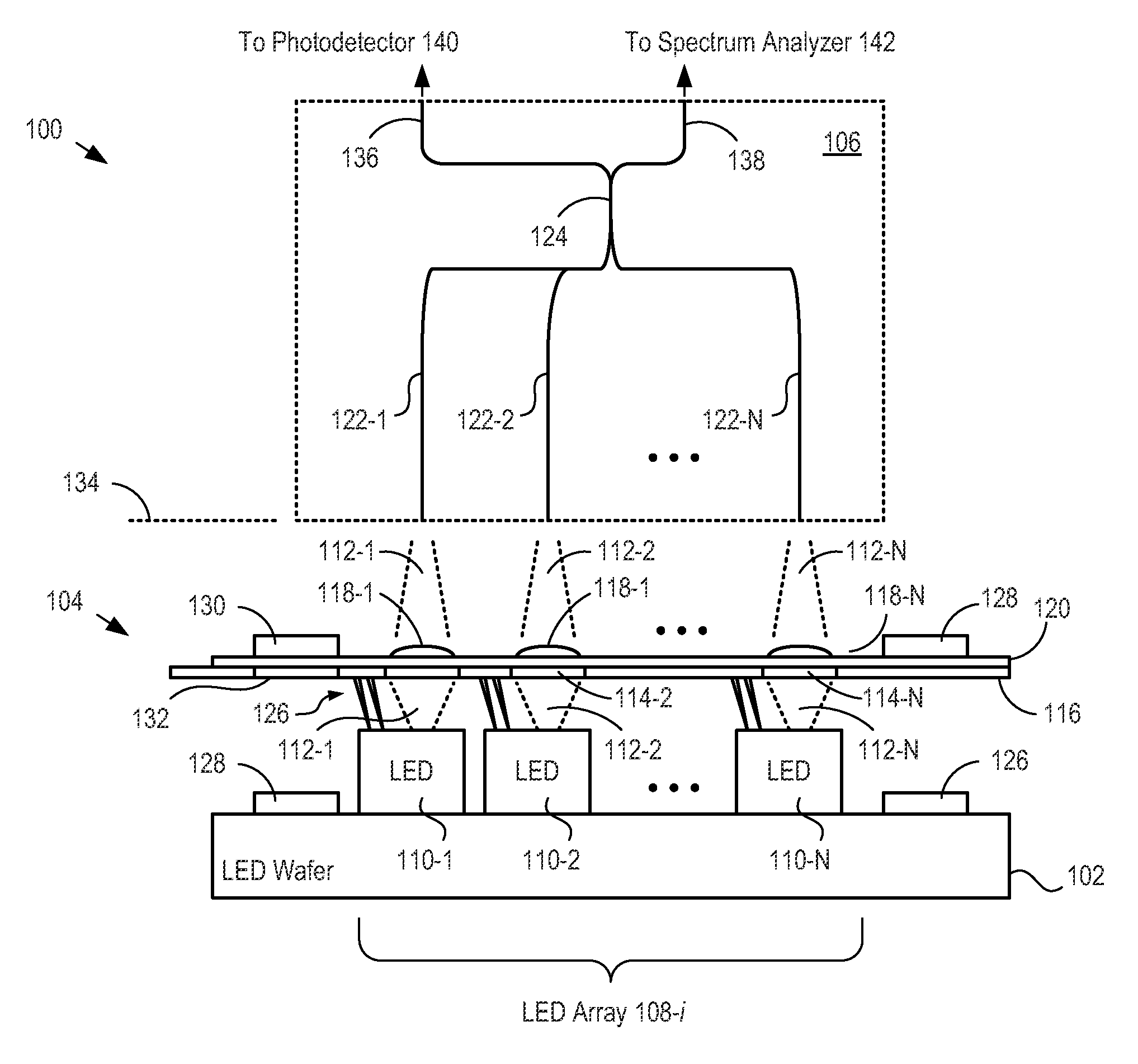
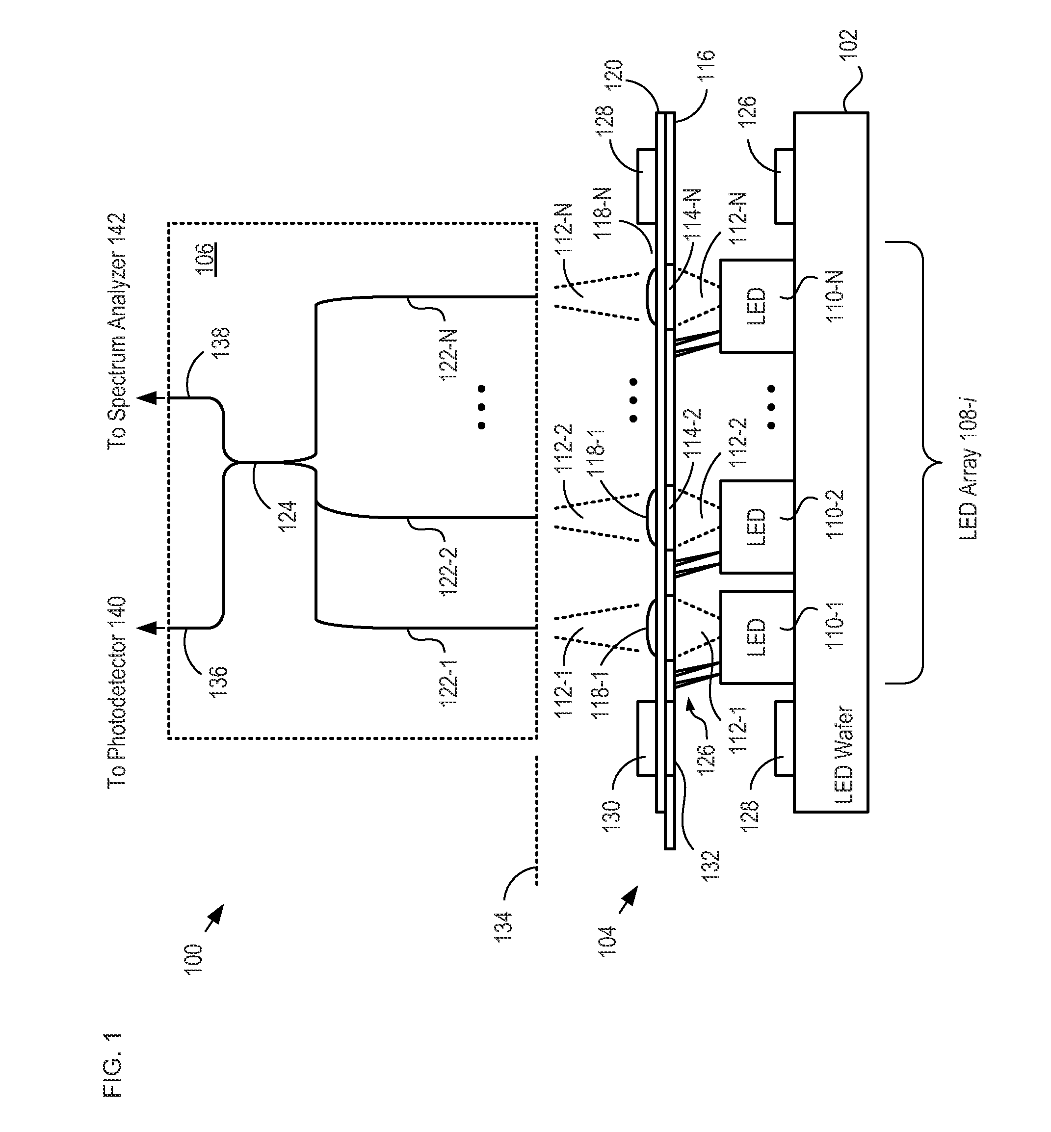
[0027]FIG. 1 depicts a probe system in accordance with an illustrative embodiment of the present invention. System 100 comprises probe card 104 and probe head 106.

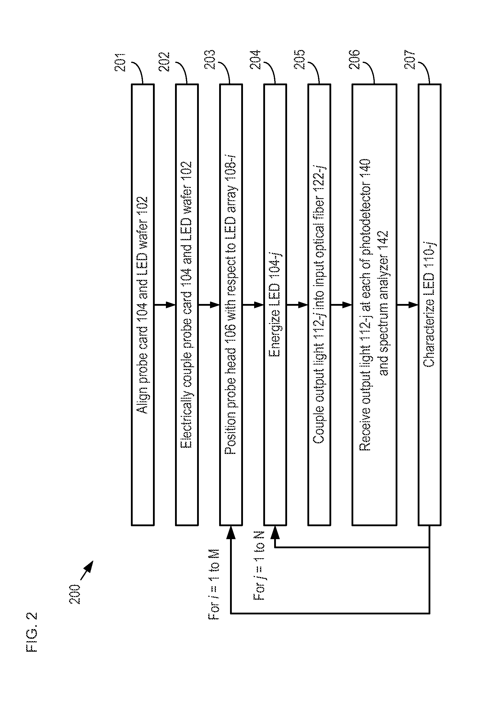
[0028]FIG. 2 depicts operations of a method suitable for use with probe system 100. Method 200 begins with operation 201, wherein probe card 104 is aligned with LED wafer 102. LED wafer 102 is a substrate comprising LEDs 110-1 through 110-N (referred to, collectively, as LEDs 110), which are LEDs suitable for lighting applications. It should be noted that, although the illustrative embodiment is described in the context of wafer-level testing LED chips, the present invention is suitable for use in the optical probing of wafers of other optoelectronic devices, such as photodetectors, lasers, VCSELs, super luminescent diodes, and the like.

[0029]Probe card 104 is a probe card that has both electrical functionality and optical functionality. Probe card 104 comprises electrical probe card 116 and lenslet plate 120. Probe card 1...


PUM


Abstract

A probe card for wafer-level testing a plurality of optoelectronic devices on a wafer is provided. The probe card has both electrical and optical functionality. The probe card comprises a plurality of lenslets aligned with the plurality of optoelectronic devices to improve the optical coupling efficiency between each of the plurality of optoelectronic devices and a plurality of optical waveguides located on a probe head.

Description

CROSS REFERENCE TO RELATED APPLICATIONS[0001]This application claims the benefit of U.S. Provisional Application Ser. No. 61 / 503,846, filed Jul. 1, 2011, entitled “Optoelectronic-Device Wafer Probe and Method Therefor,” (Attorney Docket: 882-002US), which is incorporated by reference. If there are any contradictions or inconsistencies in language between this application and one or more of the cases that have been incorporated by reference that might affect the interpretation of the claims in this case, the claims in this case should be interpreted to be consistent with the language in this case.FIELD OF THE INVENTION[0002]The present invention relates to wafer probe test fixtures for the semiconductor industry in general, and, more particularly, to wafer probe fixtures for optoelectronic device wafers.BACKGROUND OF THE INVENTION[0003]Wafer-level testing (i.e., on-wafer testing) is a critical part of high-volume production for most semiconductor devices. For electronic devices, wafe...

Claims


Application Information

Patent Timeline
IPC IPC(8): G01J1/04G01J1/44
CPCG01J2001/4247G01J1/0411G01J1/0451G01J1/0425
Inventor WALKER, JAMES ALBERT
Owner WALKER JAMES ALBERT
Why Eureka
Try Eureka