

Semiconductor device
a technology of semiconductor devices and devices, applied in semiconductor devices, semiconductor/solid-state device details, electrical apparatus, etc., can solve problems such as and achieve the effect of solving the problem of reducing the above-mentioned design window
- Summary
- Abstract
- Description
- Claims
- Application Information
AI Technical Summary
Benefits of technology
Problems solved by technology
Method used
Image

Examples
first embodiment
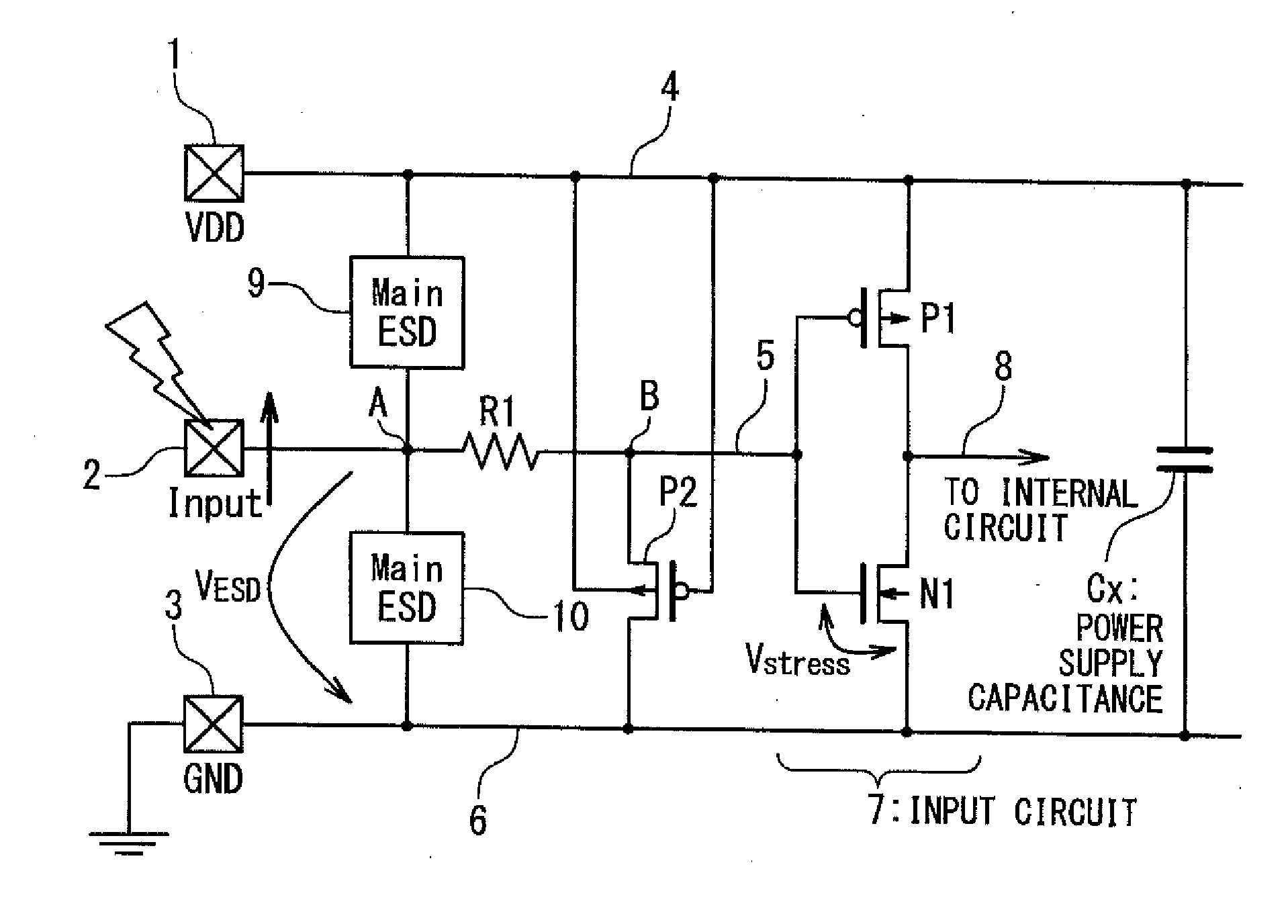
[0040]FIG. 5A is a block diagram showing a configuration of a semiconductor device according to a first embodiment of the present invention, especially, the configuration of an electrostatic protection circuit integrated in the semiconductor device. In this embodiment, the semiconductor device is provided with a power supply (VDD) pad 1, a signal input pad 2, a ground (GND) pad 3, a power supply line (a high voltage side power supply line) 4, a signal line 5 and a ground line (a low voltage side power supply line) 6. The power supply line 4 may be supplied with a power supply voltage directly from the power supply pad 1 or through a power supply node from a regulator (not shown) which is connected with the power supply pad 1. In the following description, description will be performed as use of the power supply pad 1 for both of a case of the power supply pad and a case of the power supply node. The power supply pad 1 and the ground pad 3 are connected with the power supply line 4 a...
second embodiment
[0059]FIG. 8 is a block diagram showing the configuration of the semiconductor device according to a second embodiment of the present invention. In when a further high speed operation of 10 GHz or more is considered, it is necessary in the circuit configuration of the first embodiment that a parasitic capacitance of the main ESD protection element is largely reduced and with it, the size of the main ESD protection element is reduced. In this case, there is a possibility that the discharge ability of the main ESD protection element reduces so that an excess discharge current flows into the PMOS transistor P2. In such a case, the PMOS transistor P2 which functions as the sub ESD protection element is destroyed sometimes. In order to cope with this, in the second embodiment, a technique to prevent the excess discharge current from flowing through the PMOS transistor P2 is applied to a section of the PMOS transistor P2.
[0060]More specifically, a resistance element R2 is inserted between...
third embodiment
[0061]FIG. 9A is a block diagram showing the configuration of the semiconductor device according to a third embodiment of the present invention. In the third embodiment, a diode D2 is inserted between the node B of the signal line 5 and the ground line 6 in serial with the PMOS transistor P2. The diode D2 is inserted to direct from the node B of the signal line 5 to the ground line 6 in the forward direction.
[0062]The diode D2 has a role to prevent the PMOS transistor P2 from malfunctioning when the voltage of the signal input pad 2 becomes higher because of noise and so on than that of the power supply voltage in the ordinary operation. The voltage of the signal input pad 2 is the power supply voltage at a maximum when it operates ordinarily but it sometimes exceeds the power supply voltage VDD because of noise and so on. In the configuration of the first embodiment, the malfunction that the PMOS transistor P2 is turned on in the ordinary operation can happen, when the noise level ...
PUM
 Abstract
Description
Claims
Application Information