Semiconductor device and method for manufacturing the same

a semiconductor and semiconductor technology, applied in semiconductor devices, semiconductor/solid-state device details, electrical apparatus, etc., can solve the problems of high dielectric material use method, time and material investment, bridge between lower electrodes, etc., and achieve the effect of ensuring the capacitance of capacitors

Inactive Publication Date: 2013-01-03
SK HYNIX INC
View PDF10 Cites 7 Cited by
  • Summary
  • Abstract
  • Description
  • Claims
  • Application Information

AI Technical Summary

Benefits of technology

[0008]An embodiment of the present invention relates to a semiconductor device in which a polysilicon layer of a lower electrode contact plug is removed by a strip process such that the deposition area of a dielectric film is increased and capacitance of a capacitor is guaranteed, and a method for manufacturing the same.

Problems solved by technology

Specifically, the method for using the high dielectric material requires time and material investment, for example, the introduction of new equipments or installations, the necessity of verifying the reliability and productivity of a dielectric film, low-temperature processing of a subsequent process, etc.
Specifically, the method for growing the HSG may cause unexpected problems in guaranteeing Critical Dimension (CD) of at least predetermined level between lower electrodes, and may cause a bridge between lower electrodes due to infrequent HSG desquamation, so that it is difficult for the aforementioned HSG growing method to be applied to a semiconductor device based on the design rule of 0.14 μm or less.
Provided that the cells share and use such a dielectric material, capacitance (storage capacitance) among all the lower electrodes may be deteriorated or distorted.
As a result, a bridge occurs between lower electrodes, making difficult to couple the lower electrode contact plug to the lower electrode.

Method used


Image

  • Semiconductor device and method for manufacturing the same
  • Semiconductor device and method for manufacturing the same
  • Semiconductor device and method for manufacturing the same

Examples


Embodiment Construction

[0048]Reference will now be made in detail to the embodiments of the present invention, examples of which are illustrated in the accompanying drawings. Wherever possible, the same reference numbers will be used throughout the drawings to refer to the same or like parts.

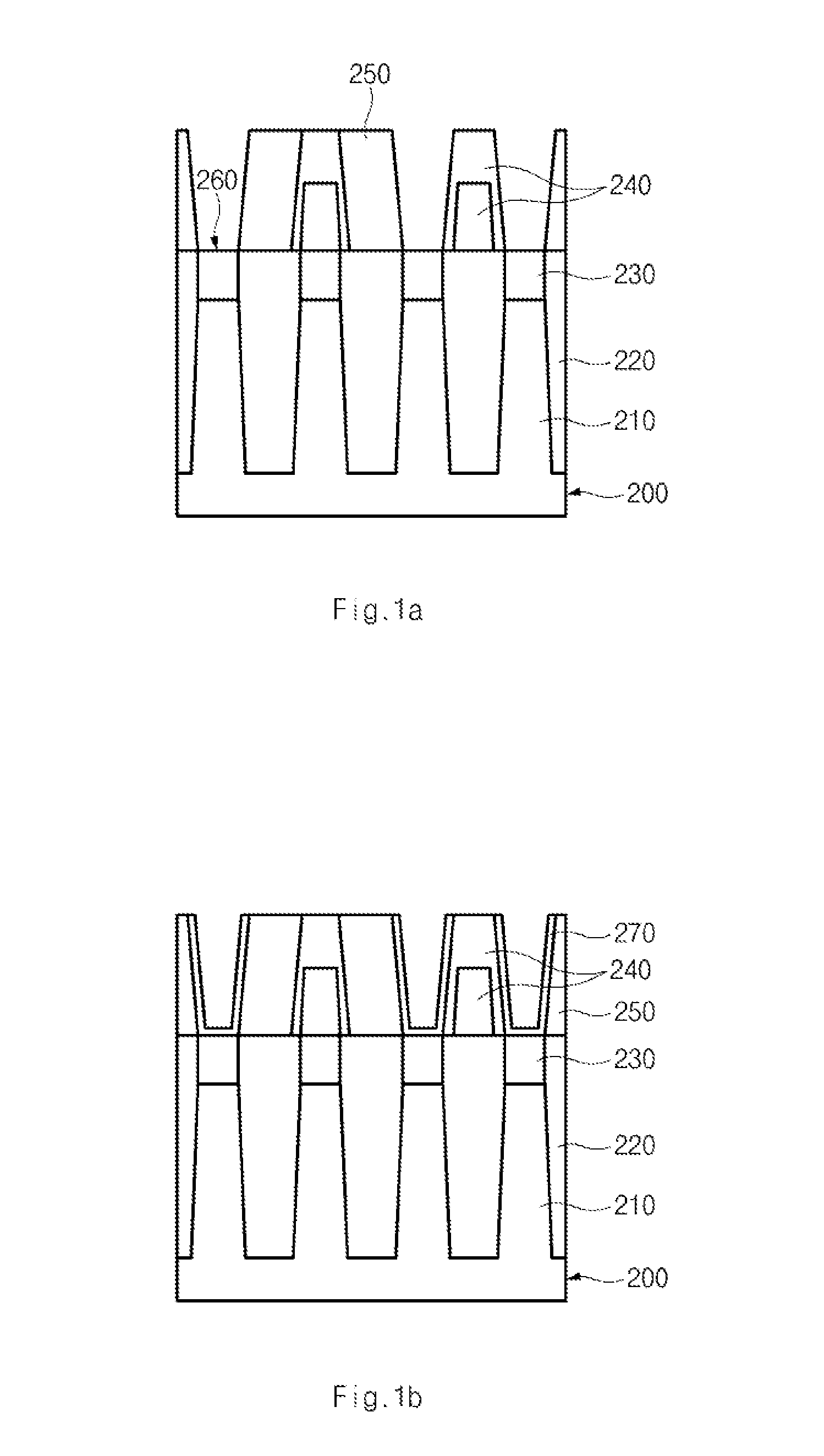
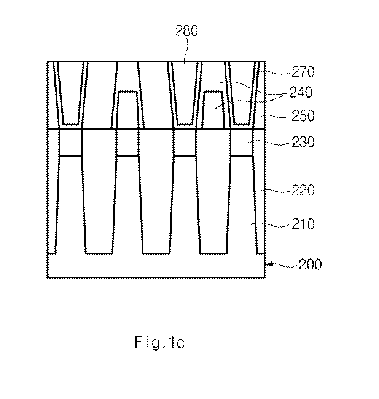
[0049]FIGS. 1a to 1h are cross-sectional views illustrating a method for manufacturing a semiconductor device according to an embodiment of the present invention.

[0050]Referring to FIG. 1a, a device isolation film 220 defining an active region 210 is formed over a semiconductor substrate 200.

[0051]Ion implantation is performed upon the top part of the active region 210 so as to form a landing plug polysilicon layer (or source / drain region) 230.

[0052]Subsequently, a bit line pattern 240 is formed over the landing plug polysilicon layer 230 and the semiconductor substrate 200. In this case, the bit line pattern 240 may be formed of a bit line metal layer and a hard mask layer. Preferably, the bit line metal layer may in...


PUM


Abstract

In a semiconductor device, a polysilicon layer of a lower electrode contact plug is removed by a strip process such that the deposition area of a dielectric film is increased and capacitance of a capacitor is assured. A method for manufacturing the semiconductor device is also disclosed.

Description

CROSS-REFERENCE TO RELATED APPLICATION[0001]The priority of Korean patent application No. 10-2011-0065682 filed on 1 Jul. 2011, the disclosure of which is hereby incorporated in its entirety by reference, is claimed.BACKGROUND OF THE INVENTION[0002]Embodiments of the present invention relate to a semiconductor device in which a polysilicon layer of a lower electrode contact plug is removed by a strip process such that the deposition area of a dielectric film is increased and capacitance of a capacitor is guaranteed, and a method for manufacturing the same.[0003]In case of a semiconductor device such as a Dynamic Random Access Memory (DRAM), it is necessary to reduce the area occupied by the semiconductor device in proportion to the increasing integration degree, and necessary electrostatic capacitance needs to be maintained or increased. Generally, there are a variety of methods to guarantee sufficient cell electrostatic capacitance within a limited area, for example, a method for u...

Claims


Application Information

Patent Timeline
Patent Type & Authority Applications(United States)
IPC IPC(8): H01L29/92
CPCH01L27/10814H01L23/5223H01L27/10885H01L27/10855H01L2924/0002H10B12/315H10B12/0335H10B12/482H01L2924/00H10B99/00H10B12/00
Inventor KIM, CHAN WOO
Owner SK HYNIX INC
Why Eureka
Try Eureka