Method of flip-chip hybridization for the forming of tight cavities and systems obtained by such a method

Inactive Publication Date: 2013-01-03
COMMISSARIAT A LENERGIE ATOMIQUE ET AUX ENERGIES ALTERNATIVES
View PDF3 Cites 1 Cited by
  • Summary
  • Abstract
  • Description
  • Claims
  • Application Information

AI Technical Summary

Benefits of technology

[0008]An object of the present invention is to provide a method for assembling two microelectronic components, which enables bo

Problems solved by technology

Although the filling material has many advantages, it cannot be applied to any type of hybridized component.
In such cases,

Method used


Image

  • Method of flip-chip hybridization for the forming of tight cavities and systems obtained by such a method
  • Method of flip-chip hybridization for the forming of tight cavities and systems obtained by such a method
  • Method of flip-chip hybridization for the forming of tight cavities and systems obtained by such a method

Examples


Example

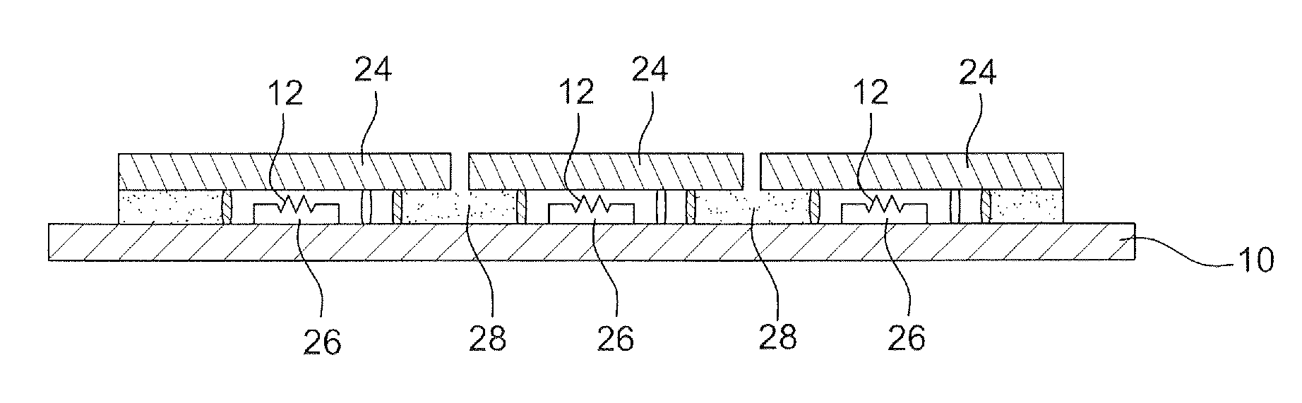
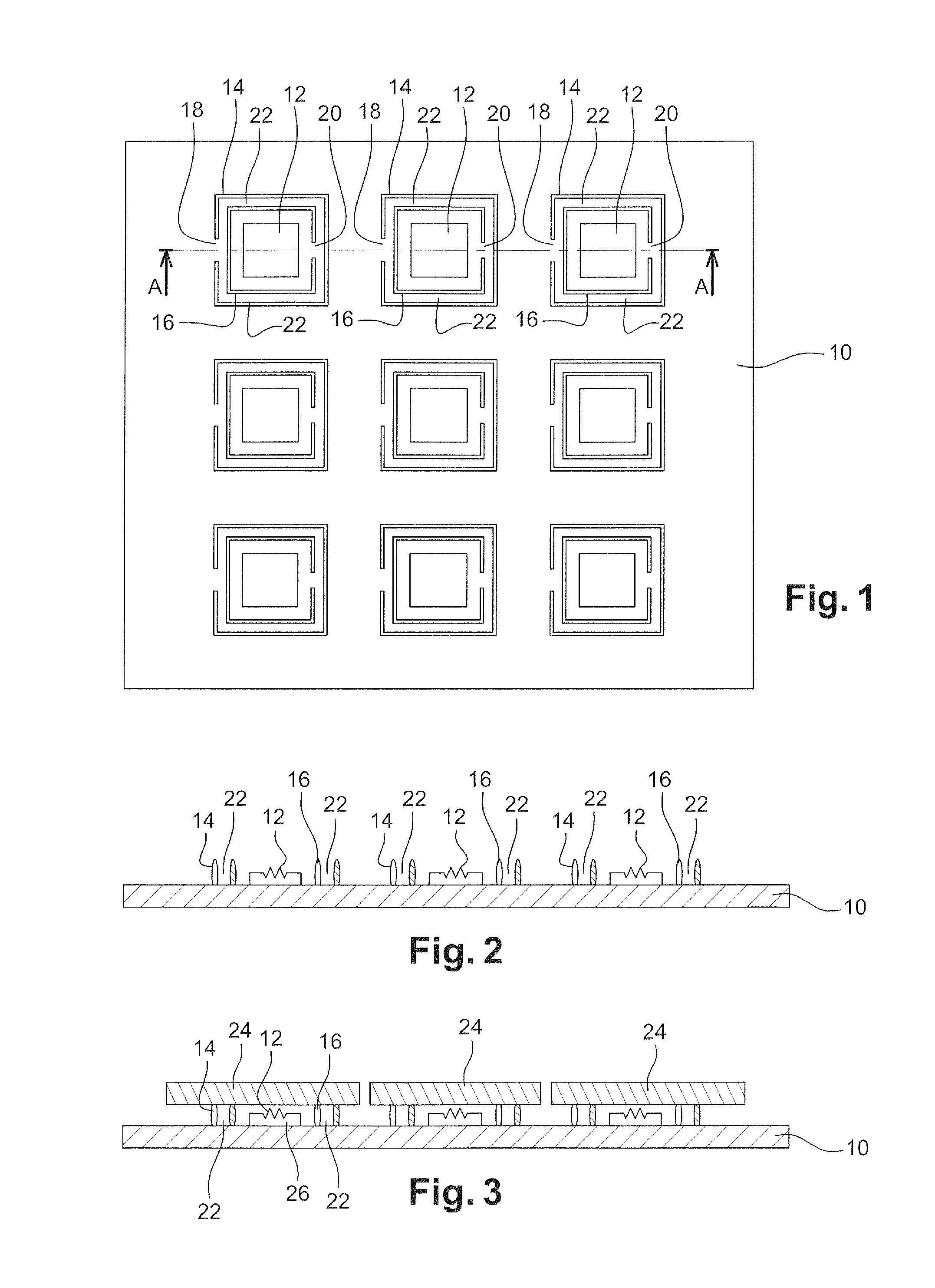
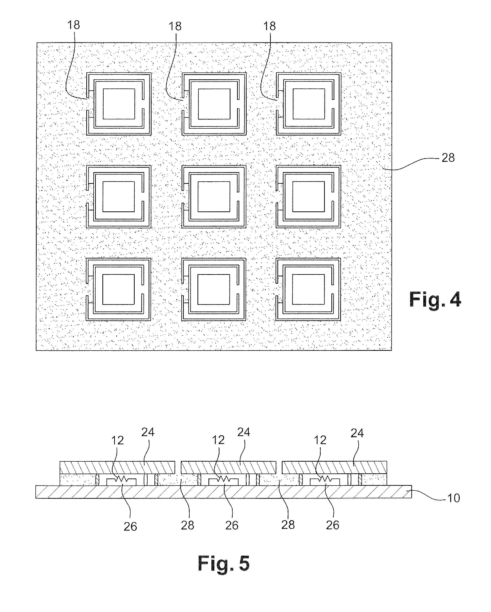
[0044]Referring to FIGS. 1 to 6, a method of an embodiment of the present invention applied to the collective forming of MEMS circuits, for example, an array of three by three MEMS circuits in the drawings, will now be described.

[0045]A circuit based on MEMSs for example comprises a substrate 10 on which or above which are formed MEMSs 12. For their operation, MEMSs 12 require being placed under low pressure, in vacuum, or under a controlled atmosphere. To achieve this, the MEMS circuits are enclosed in a tight cavity. MEMS circuits are well known per se and will not be described any further hereinafter. It should only be reminded that it is needed to provide tight cavities coated with a filling material in an underfilling operation.

[0046]As shown in FIGS. 1 and 2, the method starts with the forming of lateral walls 14, 16 around each MEMS circuit 12 to form:[0047]an external frame 14 closed except for a first vent 18; and[0048]a frame 16, internal to external frame 14, closed excep...


PUM


Abstract

A method for manufacturing a microelectronic assembly including stacked first and second microelectronic components having a cavity therebetween including defining said cavity by means of a lateral wall forming a closed frame extending around a determined area of the first component except for an opening used as a vent; forming within the closed frame and opposite to the vent an obstacle capable of forming, in cooperation with the lateral wall, a bypass duct for the filling material; performing a flip-chip hybridization of the first and second components, a surface of the second component resting on the upper edge or end of the lateral wall formed on the first component to form said at least one cavity; injecting the filling material in liquid form between the two hybridized components to embed said at least one cavity and to make it tight by obstruction of the vent as said filling material solidifies.

Description

FIELD OF THE INVENTION[0001]The present disclosure relates to the connection of two components according to the flip-chip hybridization technique.[0002]The present invention thus particularly applies to so-called “chip-on-chip”, “chip-on-wafer”, and “wafer-on-wafer” assemblies.BACKGROUND OF THE INVENTION[0003]Flip-chip hybridization is currently used to assemble two microelectronic components manufactured independently from each other, but operating complementarily, such as for example an array of unit detection elements and its read circuit, more generally by forming electromechanical connections with solder bumps or by insertion of hard metal inserts in ductile metal pads.[0004]Such hybridization is often completed by the filling of the space between the two hybridized components with a protection material, usually an epoxy resin, this operation being called underfilling.[0005]The filling material indeed enables to absorb thermal expansion differences between the first and second ...

Claims


Application Information

Patent Timeline
IPC IPC(8): H01L23/28B32B37/16
CPCH01L21/56H01L21/563H01L2924/1461H01L23/043H01L23/053H01L23/24H01L23/3121H01L23/3128H01L2224/73203H01L2924/12044B81C1/00293B81C2203/0118B81C2203/0145H01L2924/00
Inventor MARION, FRANCOIS
Owner COMMISSARIAT A LENERGIE ATOMIQUE ET AUX ENERGIES ALTERNATIVES
Why Eureka
Try Eureka