Laterally contacted blue LED with superlattice current spreading layer

a blue led, superlattice current technology, applied in the direction of electrical apparatus, semiconductor/solid-state device manufacturing, semiconductor devices, etc., can solve the problems of lattice dislocation defects of gallium nitride, and achieve the effect of facilitating current spreading, reducing current crowding, and facilitating lateral current flow

Inactive Publication Date: 2013-01-10
KK TOSHIBA
View PDF0 Cites 13 Cited by
  • Summary
  • Abstract
  • Description
  • Claims
  • Application Information

AI Technical Summary

Benefits of technology

[0006]A first function of the LRL layer is to facilitate lateral current flow underneath the n-type layer. During operation, some current flows from a part of the n-type layer, down into the LRL layer, laterally through the LRL layer, and back up into another part of the n-type layer, and to the first electrode. Such current flow through the LRL layer facilitates current spreading and reduces current crowding in the LED device.
[0007]A second function of the LRL layer is to reduce the density of lattice dislocation defects in the n-type layer and in other overlying layers in the PAN structure. In one example, the insulative substrate is a sapphire substrate, and a template layer of gallium-nitride is grown on the sapphire substrate. The LRL layer is in turn formed on the template layer. Due to different lattice constants between the sapphire material and gallium-nitride material, the gallium-nitr

Problems solved by technology

Due to different lattice constants between the sapphire material and gallium-nitride material, the

Method used


Image

  • Laterally contacted blue LED with superlattice current spreading layer
  • Laterally contacted blue LED with superlattice current spreading layer
  • Laterally contacted blue LED with superlattice current spreading layer

Examples


Embodiment Construction

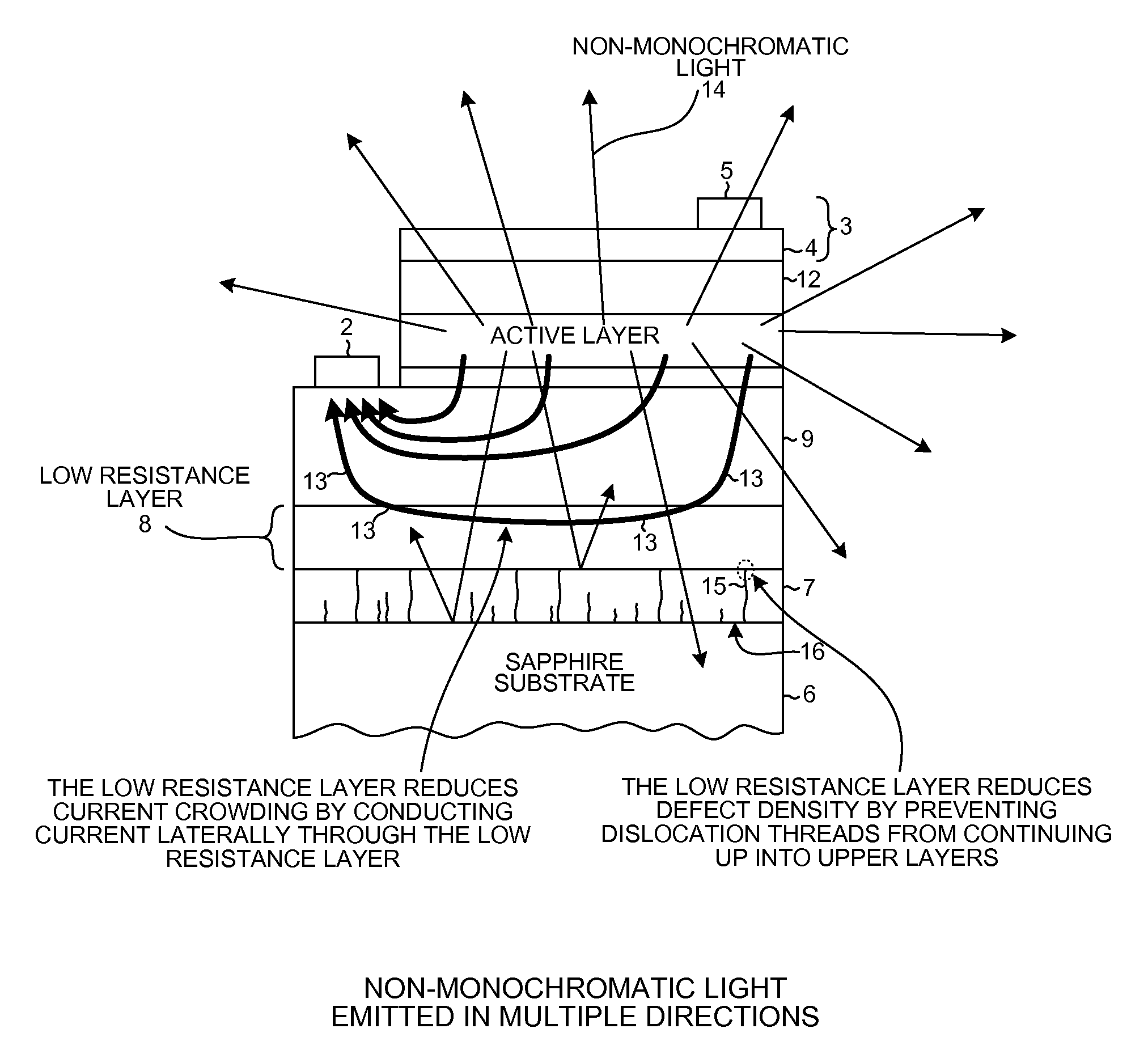
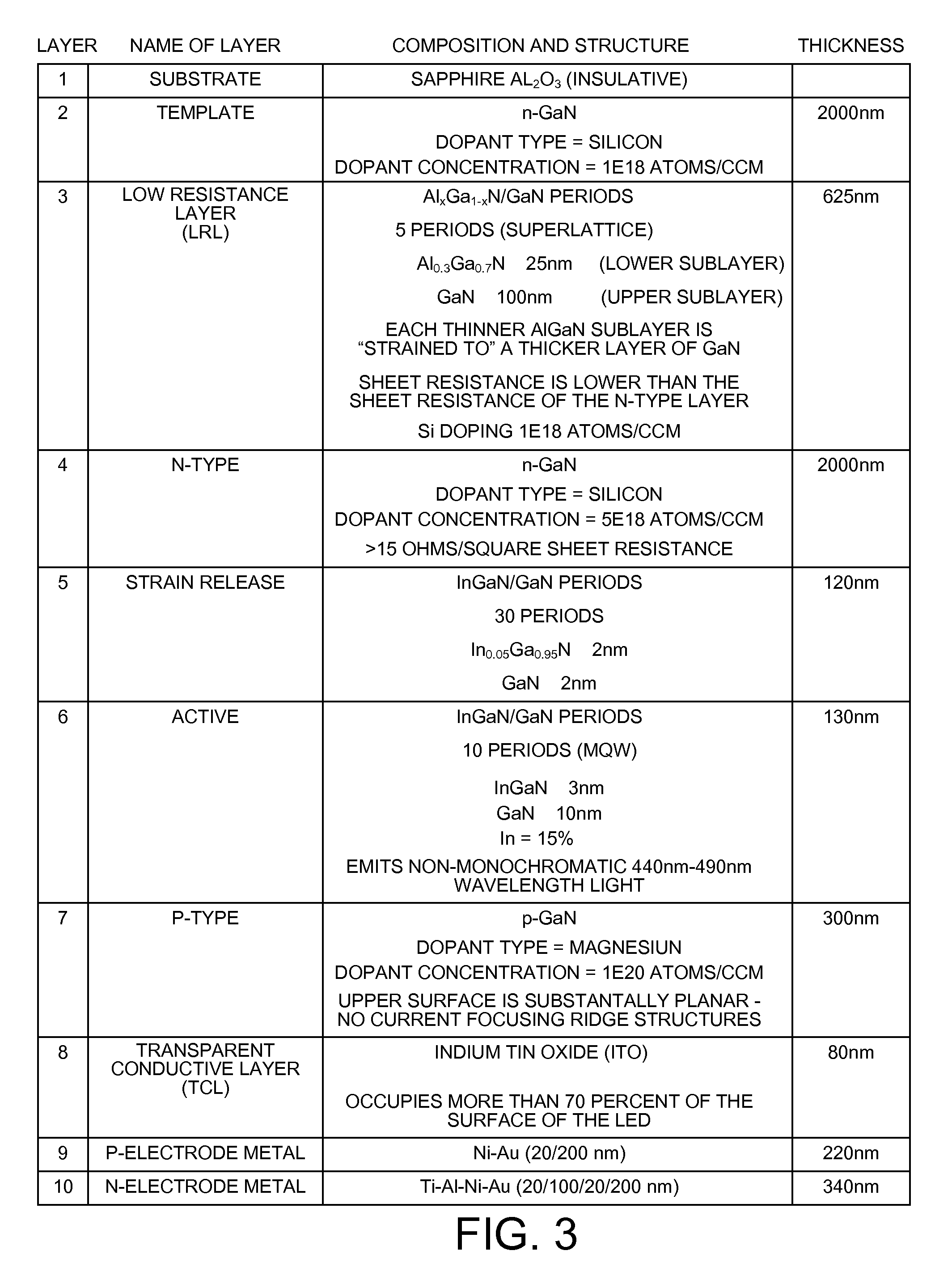
[0015]Reference will now be made in detail to some embodiments of the invention, examples of which are illustrated in the accompanying drawings. In the description and claims below, when a first layer is referred to as being disposed “over” a second layer, it is to be understood that the first layer can be directly on the second layer, or an intervening layer or layers may be present between the first and second layers. The terms such as “over”, “under”, “upper”, “lower”, “top”, “bottom”, “upward”, “downward”, “vertically”, and “laterally” are used herein to describe relative orientations between different parts of the blue LED being described, and it is to be understood that the overall blue LED structure being described can actually be oriented in any way in three-dimensional space.

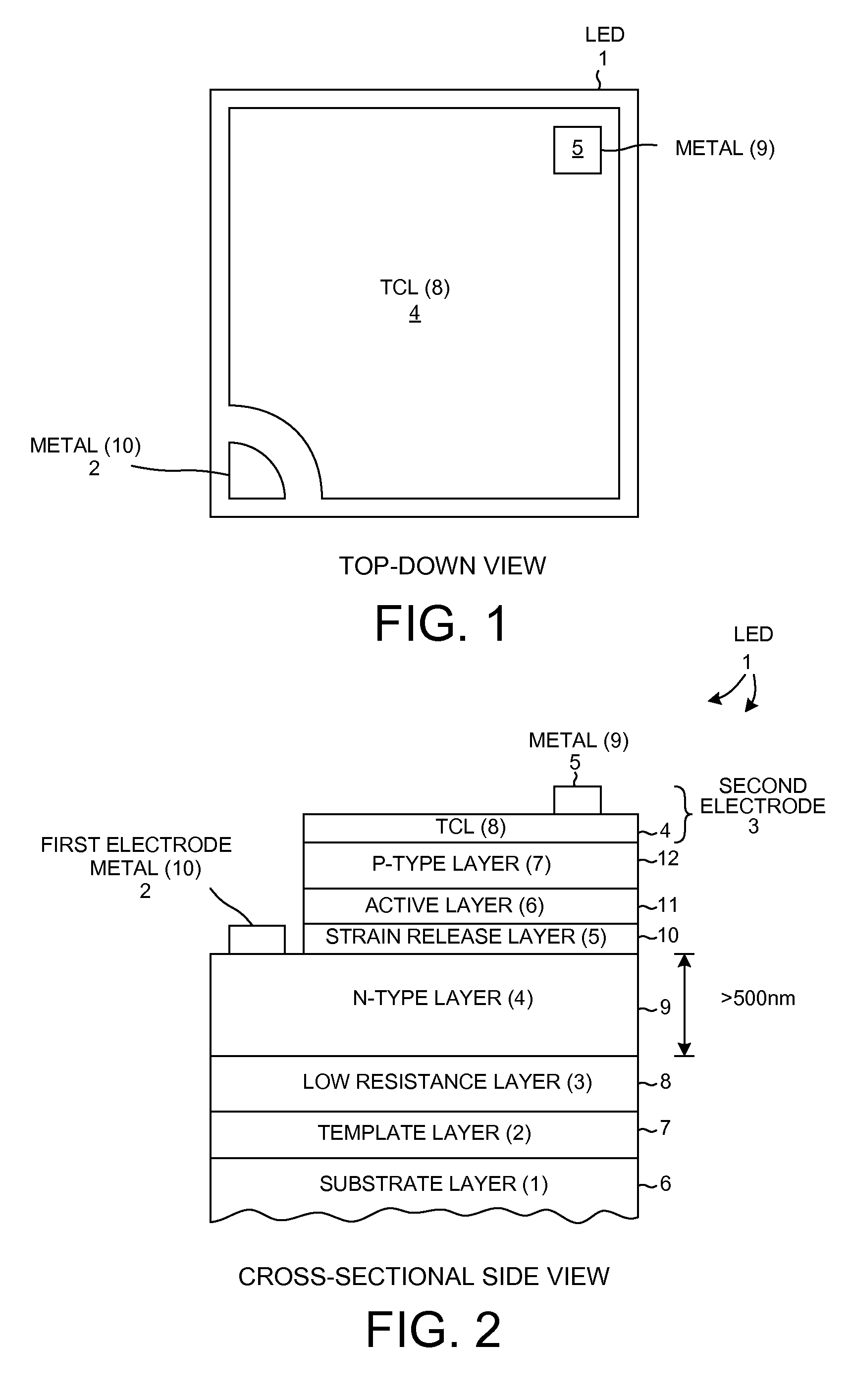
[0016]FIG. 1 is a top-down diagram of a blue Light Emitting Diode (LED) device 1 in accordance with one novel aspect. Blue LED device 1 includes a first electrode 2 and a second electrode 3. The first e...


PUM


Abstract

A laterally contacted blue LED device involves a PAN structure disposed over an insulating substrate. The substrate may be a sapphire substrate that has a template layer of GaN grown on it. The PAN structure includes an n-type GaN layer, a light-emitting active layer involving indium, and a p-type GaN layer. The n-type GaN layer has a thickness of at least 500 nm. A Low Resistance Layer (LRL) is disposed between the substrate and the PAN structure such that the LRL is in contact with the bottom of the n-layer. In one example, the LRL is an AlGaN/GaN superlattice structure whose sheet resistance is lower than the sheet resistance of the n-type GnA layer. The LRL reduces current crowding by conducting current laterally under the n-type GaN layer. The LRL reduces defect density by preventing dislocation threads in the underlying GaN template from extending up into the PAN structure.

Description

TECHNICAL FIELD[0001]The present disclosure relates generally to laterally contacted GaN-based blue LEDs.BACKGROUND INFORMATION[0002]A Light Emitting Diode (LED) is a solid state device that converts electrical energy to light. Light is emitted from an active layer of semiconductor materials sandwiched between oppositely doped layers when a voltage is applied across the doped layers. There are many different LED device structures that are made of different materials and have different structures and perform in different ways. Some emit laser light, and others generate non-monochromatic light. Some are optimized for performance in particular applications. Some are high power devices and others are not. Some emit light in infrared radiation, whereas others emit visible light of various colors, and still others emit ultraviolet light. Some are expensive to manufacture, whereas others are less expensive. For commercial general lighting applications, a so-called “laterally contacted” blu...

Claims


Application Information

Patent Timeline
IPC IPC(8): H01L33/04H01L33/02
CPCH01L33/04H01L33/32H01L33/14
Inventor CHEN, ZHENFENWICK, WILLIAMLESTER, STEVE
Owner KK TOSHIBA
Why Eureka
Try Eureka