Organic layer deposition apparatus and method of manufacturing organic light-emitting display device by using the same

a technology of organic layer and deposition apparatus, which is applied in the direction of vacuum evaporation coating, thermoelectric devices, coatings, etc., can solve the problems of difficult to achieve high light-emission efficiency with such a structure, and achieve the effects of improving manufacturing yield and deposition efficiency, simple fashion, and convenient manufacturing

Active Publication Date: 2013-01-10
SAMSUNG DISPLAY CO LTD
View PDF18 Cites 41 Cited by
  • Summary
  • Abstract
  • Description
  • Claims
  • Application Information

AI Technical Summary

Benefits of technology

[0007]Aspects of embodiments according to the present invention are directed toward an organic layer deposition apparatus that may be easily manufactured, that may be applied to the manufacture of large-size display devices on a mass scale in a simple fashion, and that improves manufacturing yield and deposition efficiency, and a method of manufacturing an organic light-emitting display device by using the organic layer deposition apparatus.

Problems solved by technology

However, it is difficult to achieve a high light-emission efficiency with such a structure, and thus intermediate layers, including an electron injection layer, an electron transport layer, a hole transport layer, a hole injection layer, and the like may be additionally interposed between the emission layer and each of the electrodes.

Method used


Image

  • Organic layer deposition apparatus and method of manufacturing organic light-emitting display device by using the same
  • Organic layer deposition apparatus and method of manufacturing organic light-emitting display device by using the same
  • Organic layer deposition apparatus and method of manufacturing organic light-emitting display device by using the same

Examples


Embodiment Construction

[0046]Reference will now be made in detail to embodiments of the present invention, examples of which are illustrated in the accompanying drawings. The invention may, however, be embodied in many different forms and should not be construed as being limited to the embodiments set forth herein; rather, these embodiments are provided so that this disclosure will be thorough and complete, and will fully convey the concept of the invention to those skilled in the art.

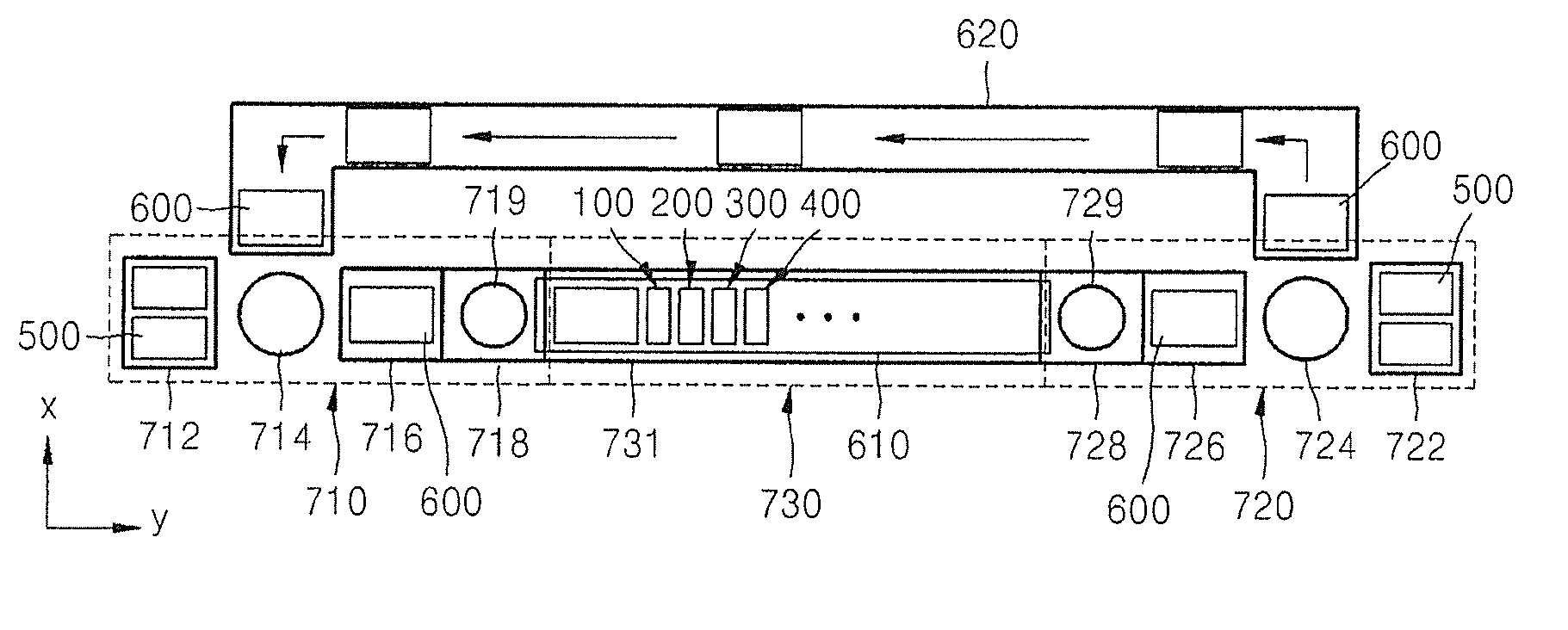
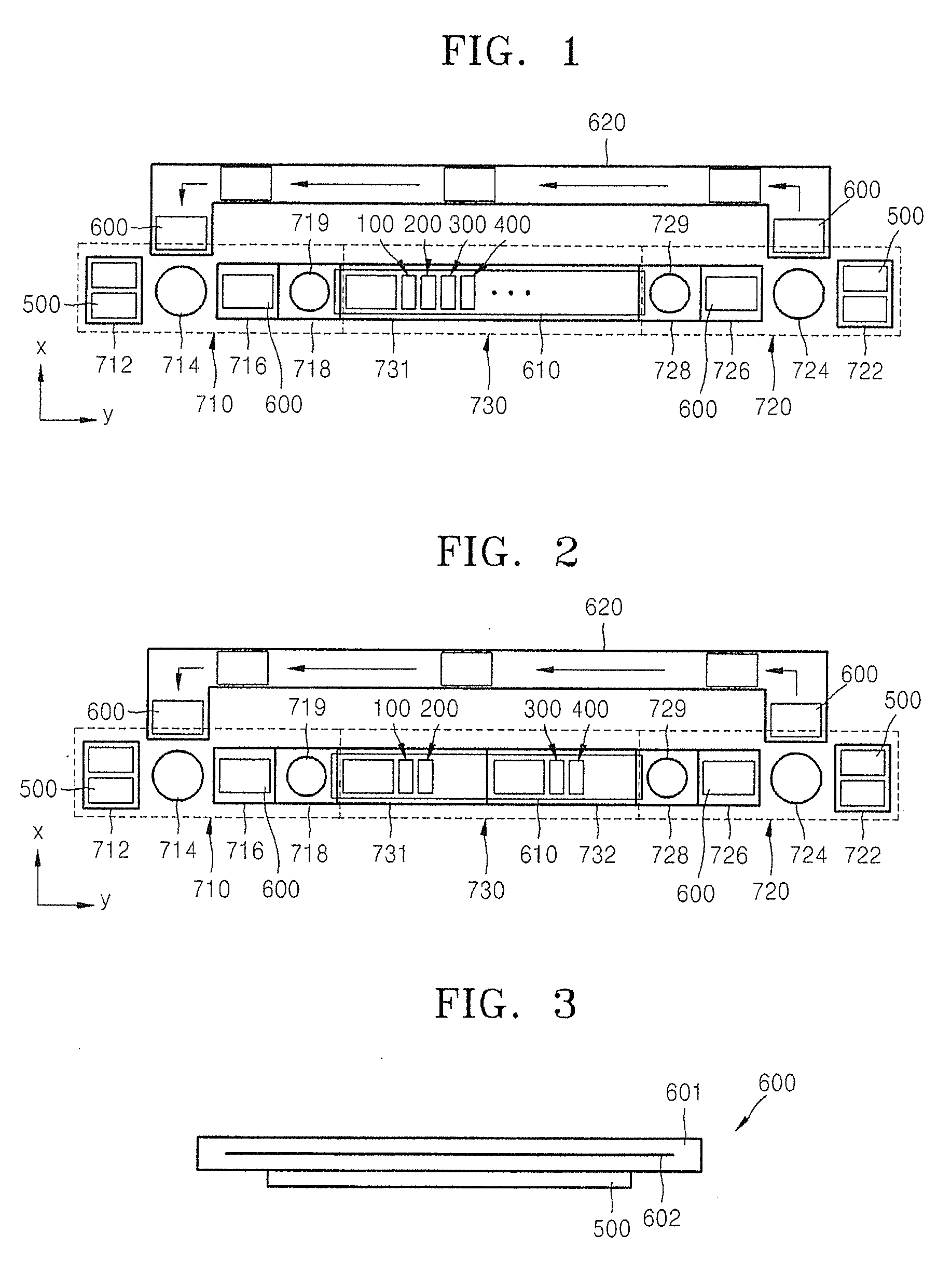
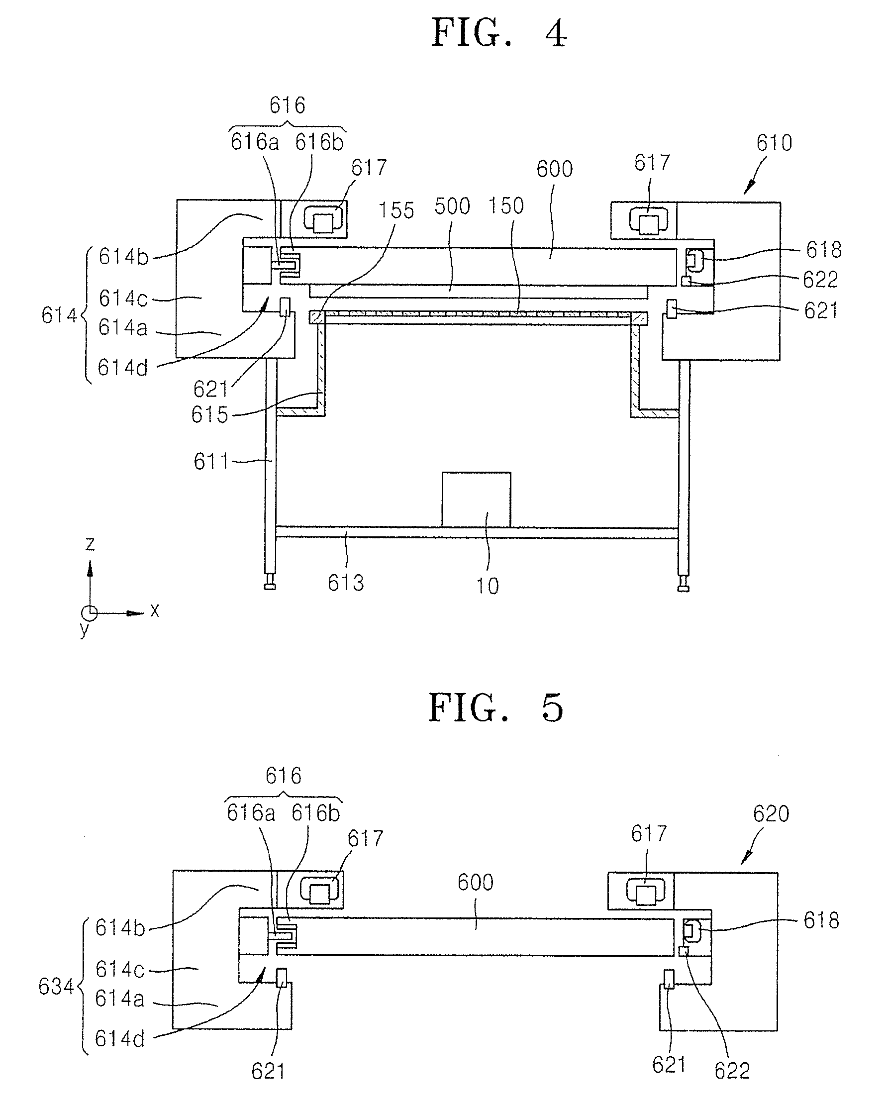
[0047]FIG. 1 is a schematic structure view of an organic layer deposition apparatus according to an embodiment of the present invention. FIG. 2 illustrates a modified example of the organic layer deposition apparatus of FIG. 1. FIG. 3 is a view of an example of an electrostatic chuck 600.

[0048]Referring to FIG. 1, the organic layer deposition apparatus according to the current embodiment includes a loading unit 710, a deposition unit 730, an unloading unit 720, a first conveyer unit 610, and a second conveyer unit 620.

[0049]...


PUM

PropertyMeasurementUnit
sizeaaaaaaaaaa
vacuumaaaaaaaaaa
driving forceaaaaaaaaaa

Abstract

An organic layer deposition apparatus, and a method of manufacturing an organic light-emitting display device using the organic layer deposition apparatus. The organic layer deposition apparatus includes: an electrostatic chuck that fixedly supports a substrate that is a deposition target; a deposition unit including a chamber maintained at a vacuum and an organic layer deposition assembly for depositing an organic layer on the substrate fixedly supported by the electrostatic chuck; and a first conveyer unit for moving the electrostatic chuck fixedly supporting the substrate into the deposition unit, wherein the first conveyer unit passes through inside the chamber, and the first conveyer unit includes a guide unit having a receiving member for supporting the electrostatic chuck to be movable in a direction.

Description

CROSS-REFERENCE TO RELATED PATENT APPLICATION[0001]This application claims priority to and the benefit of Korean Patent Application No. 10-2011-0066124, filed on Jul. 4, 2011, in the Korean Intellectual Property Office, the disclosure of which is incorporated herein in its entirety by reference.BACKGROUND[0002]1. Field[0003]Aspects of embodiments according to the present invention relate to an organic layer deposition apparatus and a method of manufacturing an organic light-emitting display device by using the same.[0004]2. Description of Related Art[0005]Organic light-emitting display devices have a larger viewing angle, better contrast characteristics, and faster response speeds than other display devices, and thus have drawn attention as next-generation display devices.[0006]Organic light-emitting display devices generally have a stacked structure including an anode, a cathode, and an emission layer interposed between the anode and the cathode. The devices display images in color...

Claims


Application Information

Patent Timeline
Patent Type & Authority Applications(United States)
IPC IPC(8): H01L51/56B05C11/00B05C13/00H01L51/52B05C15/00
CPCC23C14/12C23C14/50H01L21/67173H01L21/6831H01L21/6776H01L21/67784H01L21/67709C23C14/24H10K71/00H10K59/12H10K59/122B05B13/0221B05D1/60C23C14/042
Inventor CHANG, SEOK-RAKNAM, MYENG-WOOKANG, HEE-CHEOLKIM, JONG-HEONHONG, JONG-WONCHANG, UNO
Owner SAMSUNG DISPLAY CO LTD
Why Eureka
Try Eureka