
Device and Method For Buffer-Storing A Multiplicity of Wafer-Type Workpieces

a technology of multiplicity and workpiece, applied in the direction of loading/unloading, thin material handling, article separation, etc., can solve the problems of increasing the cost of operating personnel, not being able to use batch cleaning methods, semiconductor wafers,

Active Publication Date: 2013-01-10
SILTRONIC AG
View PDF10 Cites 18 Cited by
  • Summary
  • Abstract
  • Description
  • Claims
  • Application Information

AI Technical Summary

Benefits of technology

The invention allows for efficient and space-saving processing of workpieces. It allows for fast and easy stacking of workpieces during processing and easy removal of them in the correct order. This eliminates the need for a horizontal transport system and reduces space requirements. It also allows for faster and more accurate manual loading of the workpieces. Overall, the invention increases efficiency and flexibility in processing.

Problems solved by technology

Preferably, the cleaning is effected directly after the preceding lapping, grinding or polishing processing, as long as the semiconductor wafers are still wet, since lapping or polishing agent or grinding slurry, once it has dried in, adheres very strongly to the surface or even damages the latter.
However, these methods always operate with cyclic or continuous passage of individual semiconductor wafers, since each surface of each semiconductor wafer fed for cleaning has to be swept over completely by a cleaning tool.
This is not possible in batch cleaning methods.
Consequently, in many cases there is the problem that semiconductor wafers obtained in bunches after processing in a batch process have to be separated and fed for cleaning successively cyclically or with continuous passage.
Furthermore, for reasons of economic viability, it is undesirable that, for example, the installation operator who unloads the semiconductor wafers after processing by a batch process and feeds them manually for subsequent cleaning adapts his unloading pace to the cleaning throughput, since this leads to waiting times, increased outlay on operating personnel, reduced material throughput and quality losses.
Quality losses can arise in the case of DSP, for example, if polishing agent adhering to the surface of the semiconductor wafer dries thereon.
Therefore, it is not possible, in particular, to pick up a plurality of semiconductor wafers within a short time from a preceding batch processing process and to simultaneously remove them individually again successively in time with the subsequent cleaning and in the order of inclusion in the stack (“first in first out” principle, FIFO).
Moreover, the buffer store described in JP2006-032528A also does not permit fast direct loading by hand, for example by an installation operator who removes the semiconductor wafers after the end of the preceding batch processing process rapidly, successively and in a manner maintaining the order from the processing device, since loading takes place by means of the transport rollers through between the sprockets.
The workpieces would additionally have to be placed onto the moving transport rollers, which would inevitably lead to undesirable friction between transport rollers and workpiece.
Moreover, the lateral loading necessitates an additional space requirement of such a device, as a result of which it cannot simply be attached to the processing device that supplies the semiconductor wafers, or it cannot easily be retrofitted if necessary without in general having to shift and rearrange the processing device.
In many cases it is even completely impossible to shift the processing device, since, in modern manufacturing sequences, in general a multiplicity of different processing devices are installed at small distances from one another or in predefined building grids, the arrangement of which can no longer be changed subsequently without disturbing the entire processing sequence in the long term or changing it permanently.

Method used


Image

  • Device and Method For Buffer-Storing A Multiplicity of Wafer-Type Workpieces
  • Device and Method For Buffer-Storing A Multiplicity of Wafer-Type Workpieces
  • Device and Method For Buffer-Storing A Multiplicity of Wafer-Type Workpieces

Examples


example

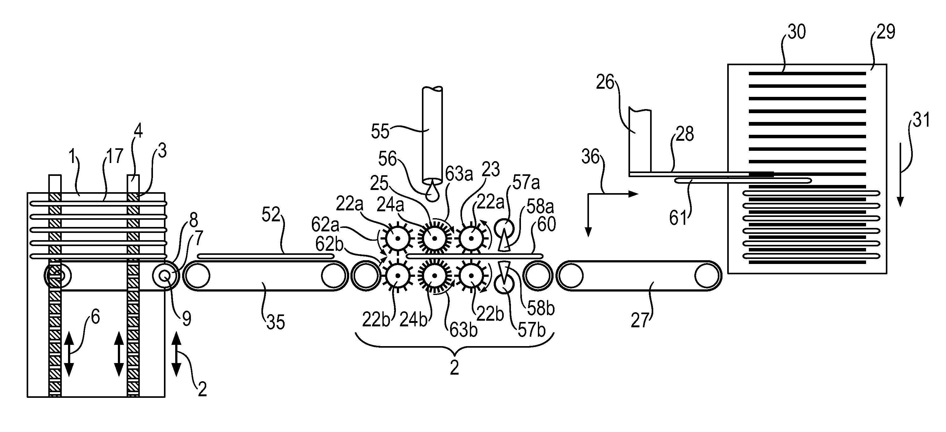
[0103]A buffer-storing, cleaning and tray introducing device embodied in accordance with FIG. 6 was operated for cleaning semiconductor wafers from preceding processing by the PPG method. The pure grinding time was approximately 4 minutes during the PPG processing. For loading a PPG batch of 15 semiconductor wafers having a diameter of 300 mm, the installation operator needed approximately 90 seconds; and approximately 120 seconds for unloading. Including ancillary times of the installation (pivoting, lifting and lowering of the upper working disk at the beginning and end of the process; positioning the carriers with the semiconductor wafers after the end of the pass, such that the carrier loaded first was the first to pass into the unloading position after the end of the pass, and removing semiconductor wafers possibly adhering to the upper working disk after the end of the pass), the cycle time was approximately 9.5 minutes. The buffer store was operated with the first method acco...


PUM


Abstract

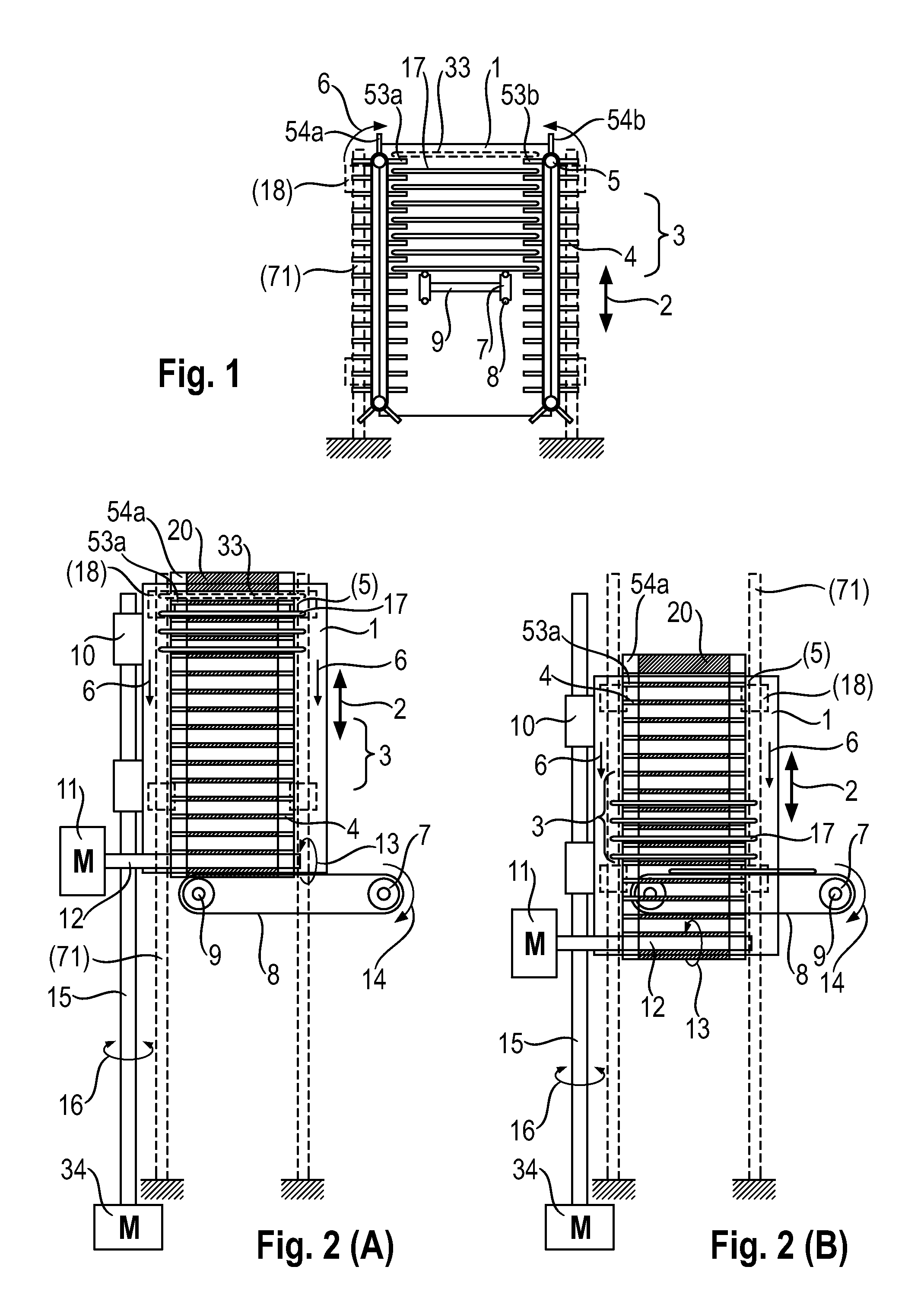
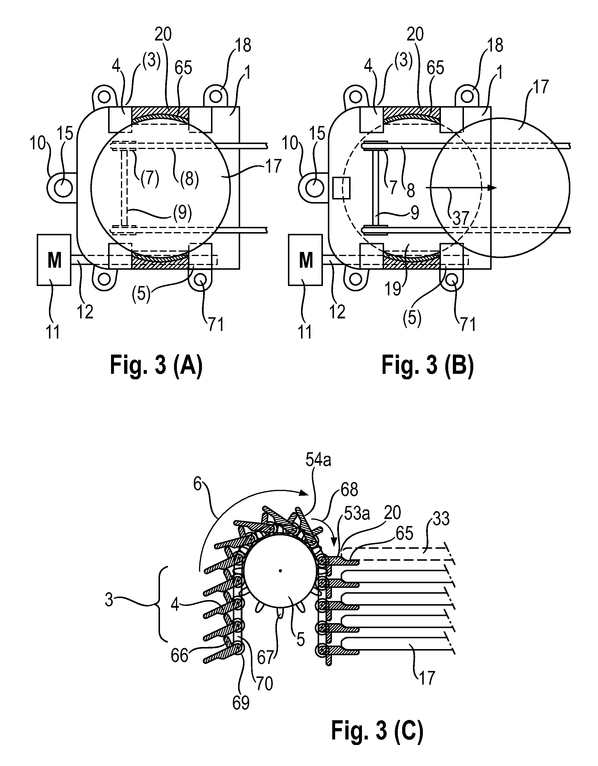
A multiplicity of wafer-type workpieces are buffer stored in a device having,a frame,at least two transport elements which each circulate in a vertical direction around an upper and a lower deflection device connected to the frame and are provided, at uniform intervals, with a multiplicity of bearing areas for the horizontal mounting of workpieces, wherein at least one of the deflection devices of each transport element is driven and a free space is situated between the transport elements,a loading position between the upper deflection devices at which a workpiece can be placed onto corresponding bearing areas, anda stationary removal device below the loading position, comprising a horizontal transport device, the first end of which lies within the free space between the transport elements. The invention also relates to a method for buffer-storing a multiplicity of wafer-type workpieces using the abovementioned device.

Description

CROSS-REFERENCE TO RELATED APPLICATIONS[0001]This application claims priority to German Patent Application No. DE 102011078614.7 filed Jul. 4, 2011 which is herein incorporated by reference.BACKGROUND OF THE INVENTION[0002]1. Field of the Invention[0003]The present invention relates to a device and a method for buffer-storing a multiplicity of wafer-type workpieces vertically one above another and individually without the workpieces touching one another. The device comprises a frame, at least two transport elements which circulate in a vertical direction and which are provided, at uniform intervals, with a multiplicity of bearing areas for the horizontal mounting of workpieces, a loading position and a stationary removal device.[0004]2. Background Art[0005]Various products in modern industry require semifinished products in the form of very precisely processed wafer-type workpieces. These are, for example, annular wafers composed of glass or aluminum as substrates for the production...

Claims


Application Information

Patent Timeline
Patent Type & Authority Applications(United States)
IPC IPC(8): B65G1/04H01L21/677
CPCB65G47/5127H01L21/67778H01L21/67769B65G1/127B65G65/00B65G1/12Y10S414/137
Inventor PIETSCH, GEORG
Owner SILTRONIC AG
Learn More