Die-Sized Atomic Magnetometer and Method of Forming the Magnetometer

a magnetometer and atomic magnetometer technology, applied in the field of atomic magnetometers, can solve the problems of limiting the types of applications where atomic magnetometers can be commercially utilized, and the ability of electrons to no longer absorb light energy,

Active Publication Date: 2013-01-17
NAT SEMICON CORP
View PDF3 Cites 25 Cited by
  • Summary
  • Abstract
  • Description
  • Claims
  • Application Information

AI Technical Summary

Problems solved by technology

When the electron falls back to the highest energy level that is associated with the outer shell, the electron is no longer capable of absorbing any light energy.
Two of the drawbacks of conventional atomic magnetometers are size and cost, which then limit the types of applications where atomic magnetometers can be commercially utilized.

Method used


Image

  • Die-Sized Atomic Magnetometer and Method of Forming the Magnetometer
  • Die-Sized Atomic Magnetometer and Method of Forming the Magnetometer
  • Die-Sized Atomic Magnetometer and Method of Forming the Magnetometer

Examples


Embodiment Construction

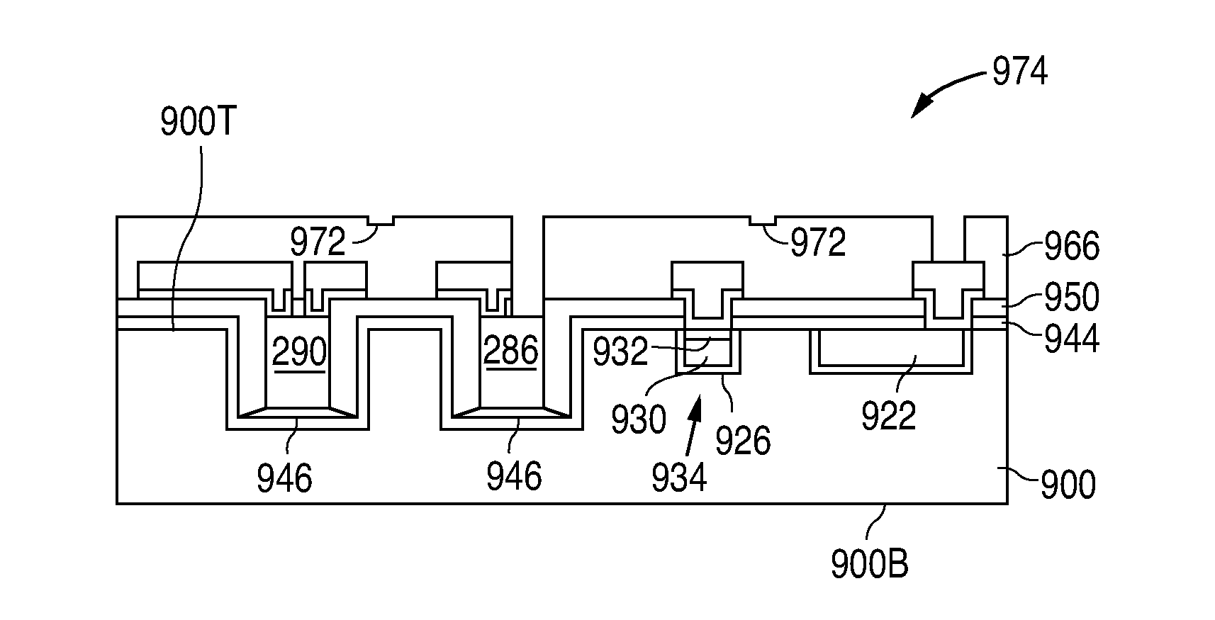
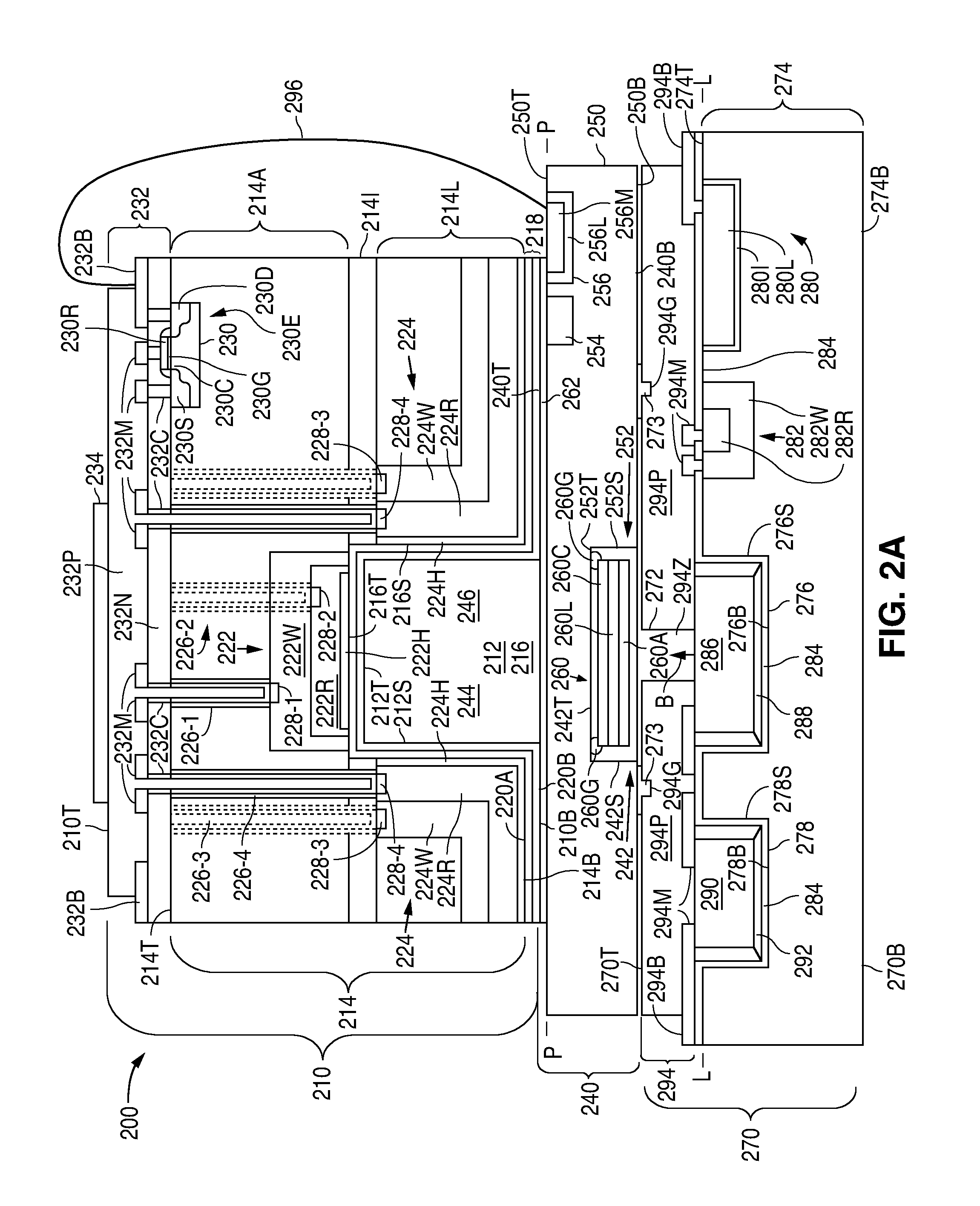
[0026]FIG. 2A shows a cross-sectional view that illustrates an example of a die-sized atomic magnetometer 200 in accordance with the present invention. As shown in FIG. 2A, atomic magnetometer 200 includes a first die 210 that has a top surface 210T, a bottom surface 2106, and a first die cavity 212 that extends into first die 210 from the bottom surface 210B of first die 210. First die cavity 212, in turn, has a top surface 212T and a side wall surface 212S. The top surface 212T of first die cavity 212 lies below and spaced apart from the top surface 210T of first die 210.

[0027]As further shown in FIG. 2A, first die 210 includes a first semiconductor structure 214 that has a top surface 214T, a bottom surface 214B, and a first semiconductor cavity 216 that extends into first semiconductor structure 214 from the bottom surface 214B of first semiconductor structure 214. First semiconductor cavity 216, in turn, has a top surface 216T and a side wall surface 216S. The top surface 216T ...


PUM

PropertyMeasurementUnit
wavelengthaaaaaaaaaa
thicknessaaaaaaaaaa
thicknessaaaaaaaaaa

Abstract

The cost and size of an atomic magnetometer are reduced by attaching together a first die which integrates together a vapor cell, top and side photo detectors, and processing electronics, a second die which integrates together an optics package and a heater for the vapor cell, and a third die which integrates together a VCSEL, a heater for the VCSEL, and control electronics.

Description

BACKGROUND OF THE INVENTION[0001]1. Field of the Invention[0002]The present invention relates to atomic magnetometers and, more particularly, to a die-sized atomic magnetometer and a method of forming the magnetometer.[0003]2. Description of the Related Art[0004]An atomic magnetometer is a device that measures the strength of a magnetic field by determining a frequency known as the Larmor frequency. The Larmor frequency, in turn, is the frequency of the magnetic moment of a contained group of in-phase spinning alkali atoms moving in precession in response to the magnetic field. A magnetic field strength B is defined by the equation B=hvL / γ, where h is Plank's constant, hvL is the Larmor frequency, and γ is the gyromagnetic ratio (e.g., 7 Hz / nT for 87Rb and 3.5 Hz / nT for Cs).[0005]FIG. 1 shows a block diagram that illustrates an example of a prior art atomic magnetometer 100. As shown in FIG. 1, atomic magnetometer 100 includes a vertical cavity surface emitting laser (VCSEL) 110, an...

Claims


Application Information

Patent Timeline
Patent Type & Authority Applications(United States)
IPC IPC(8): G01R33/02H01L43/12H01L31/02G01N21/59H01L29/02H01L21/50H01S3/02G01J1/42H01L29/82H01L31/18
CPCG01R33/032H01S5/026H01S5/0261G01J1/4228G01J1/44G01J5/20H01S5/183H01L2224/04105H01L2224/73267H01L2224/92244H01L2224/19H01L2224/32145H01L2224/82H01L2924/15153H10N50/01G01R33/0052H01L31/18H01S5/0208H01S5/0222H01S5/0262H01L2224/18H01L2224/32225
Inventor LINDORFER, PHILIPPHOPPER, PETER J.FRENCH, WILLIAMMAWSON, PAULHUNT, STEVENPARSA, ROOZBEH
Owner NAT SEMICON CORP
Why Eureka
Try Eureka