Touch panel integrated display device and method for manufacturing the same

Inactive Publication Date: 2013-01-17
ALPS ALPINE CO LTD
View PDF7 Cites 67 Cited by
  • Summary
  • Abstract
  • Description
  • Claims
  • Application Information

AI Technical Summary

Benefits of technology

[0032]In the step of (a), the adhesive layer may preferably be an ultraviolet-curable resin layer. Thus, since the step of

Problems solved by technology

In this case, electromagnetic noise from the liquid crystal panel 130 may become background noise during an input operation and degrade the signal-to-noise (S/N) ratio, or even cause malfunction of the touch panel 110.
This makes it difficult to reduce the overall thickness of the display device.
This is disadvantageous in reducing the thickness of the display device.
The double-sided film deposition step req

Method used


Image

  • Touch panel integrated display device and method for manufacturing the same
  • Touch panel integrated display device and method for manufacturing the same
  • Touch panel integrated display device and method for manufacturing the same

Examples


first embodiment

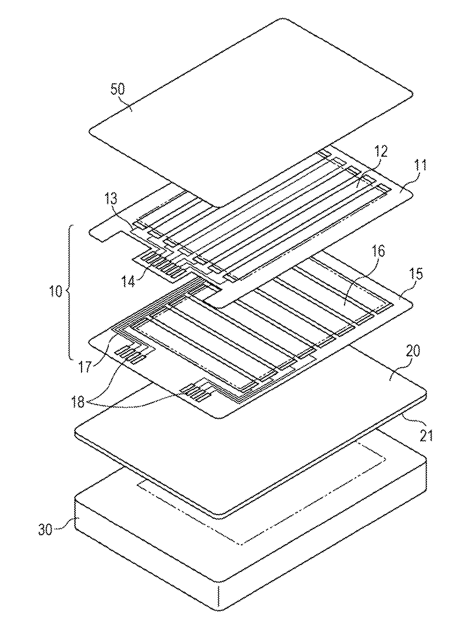
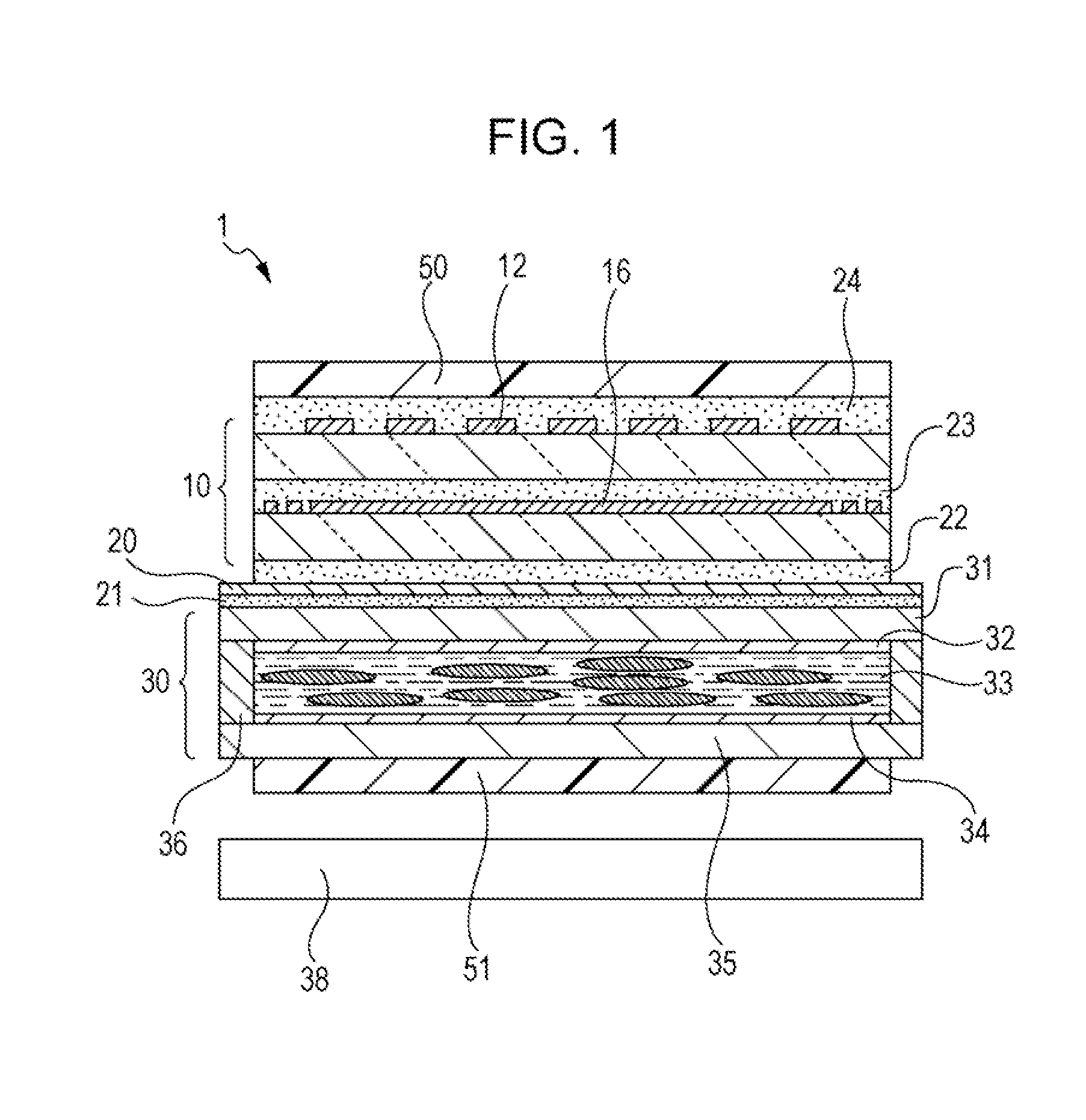
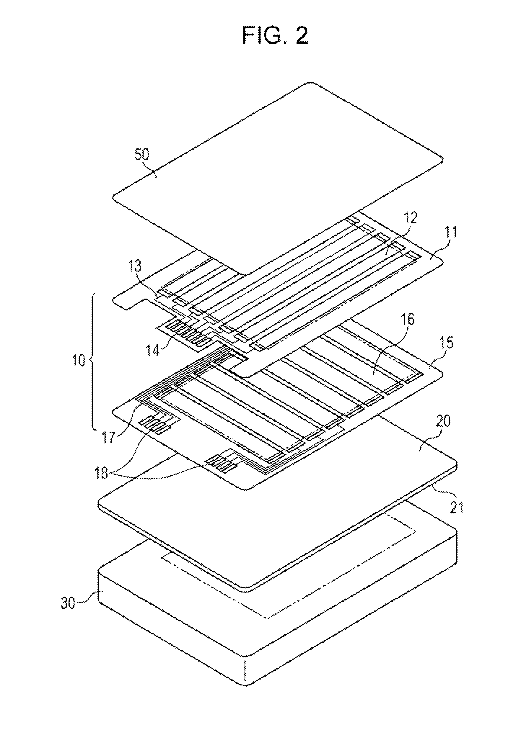
[0052]FIG. 1 is a cross-sectional view of a touch panel integrated display device 1 according to a first embodiment. FIG. 2 is an exploded perspective view of the touch panel integrated display device 1. Note that dimensions in each drawing are changed as necessary for visibility.

[0053]As illustrated in FIG. 1, in the touch panel integrated display device 1 of the present embodiment, a liquid crystal panel 30 is used as a display panel that displays images and text information. A capacitive touch panel 10 serving as a light-transmissive touch panel is disposed on a display side of the liquid crystal panel 30. Through the touch panel 10, the operator can view images from the liquid crystal panel 30. The operator can thus perform an input operation on the touch panel 10 while viewing displayed images and menus.

[0054]A transparent conductive layer 20 is formed by transfer onto the display surface of the liquid crystal panel 30, with an adhesive layer 21 interposed therebetween. The tra...

second embodiment

[0085]FIG. 5 is a cross-sectional view of a touch panel integrated display device 2 according to a second embodiment. The same components as those of the first embodiment are given the same reference numerals.

[0086]In the present embodiment, an OLED panel 40 is used as a display panel that displays images and text information. The transparent conductive layer 20 for suppressing electromagnetic noise is formed by transfer onto the display surface of the OLED panel 40, with the adhesive layer 21 interposed therebetween. The touch panel 10 is bonded to the transparent conductive layer 20, with the sticky layer 22 interposed therebetween.

[0087]The OLED panel 40 includes a plurality of light-emitting function layers 43, each formed by stacking a positive-hole transport layer, a light emitting layer, and an electron injection layer (not shown). The light-emitting function layers 43 include light-emitting function layers 43a that emit red light, light-emitting function layers 43b that emit...

third embodiment

[0092]FIG. 7 is a cross-sectional view of a touch panel integrated display device 3 according to a third embodiment. FIG. 8 is an exploded perspective view of the touch panel integrated display device 3.

[0093]The touch panel integrated display device 3 illustrated in FIG. 7 includes a touch panel 70, instead of the touch panel 10 of the touch panel integrated display device 1 of the first embodiment illustrated in FIG. 1. Except for the touch panel 70, the structure of the touch panel integrated display device 3 illustrated in FIG. 7 is the same as that of the touch panel integrated display device 1 illustrated in FIG. 1.

[0094]The touch panel 70 is formed by arranging first electrode layers 72 and second electrode layers 73 only on an input side of a transparent base 71. The transparent base 71 is made of flexible film material. For example, a PET film is used as the transparent base 71. The first electrode layers 72 and the second electrode layers 73 are made of transparent conduct...


PUM

PropertyMeasurementUnit
Electrical conductoraaaaaaaaaa
Transparencyaaaaaaaaaa
Phaseaaaaaaaaaa

Abstract

A method for manufacturing a touch panel integrated display device including a touch panel and a display panel that are integrally stacked, with a light-transmissive sticky layer interposed therebetween, includes the steps of (a) forming a transparent conductive layer by transfer onto a display surface of the display panel, with an adhesive layer interposed therebetween, by using a transferable film having the adhesive layer and the transparent conductive layer; (b) stacking a polarizing layer on one surface of the touch panel, the one surface being an input surface of the touch panel; and (c) bonding the transparent conductive layer formed on the display surface of the display panel to the other surface of the touch panel, with the sticky layer interposed therebetween.

Description

CLAIM OF PRIORITY[0001]This application claims benefit of Japanese Patent Application No. 2011-156712 filed on Jul. 15, 2011 and No. 2012-000829 filed on Jan. 5, 2012, which are hereby incorporated by reference.BACKGROUND OF THE INVENTION[0002]1. Field of the Invention[0003]The present invention relates to touch panel integrated display devices and methods for manufacturing the same. In particular, the present invention relates to a touch panel integrated display device and a method for manufacturing the same that can suppress electromagnetic noise from a display panel, reduce the device thickness, and lower the manufacturing costs.[0004]2. Description of the Related Art[0005]In an operation unit of electronic equipment, such as mobile equipment, a display device is often used which includes a touch panel disposed on a display side of a display panel, such as a liquid crystal panel or an organic light-emitting diode (OLED) panel. A touch panel is a light-transmissive input unit whic...

Claims


Application Information

Patent Timeline
IPC IPC(8): G06F3/041B32B37/12
CPCG02F1/13338G06F3/044Y10T156/10G06F2203/04103G02F2001/133334G06F3/0446G06F3/0445G02F1/133334G06F3/0412G02F1/133528G02F1/13363H10K59/40
Inventor MASUMOTO, YOSHIFUMI
Owner ALPS ALPINE CO LTD
Why Eureka
Try Eureka