Method of inspecting mask, mask inspection device, and method of manufacturing mask

a mask inspection and mask technology, applied in the direction of photomechanical treatment originals, optical radiation measurement, instruments, etc., can solve the problems of reduced transparency of scattered light, and reduced detection sensitivity of phase defects, so as to increase the background level of inspection signals and reduce detection sensitivity

Active Publication Date: 2013-01-17
RENESAS ELECTRONICS CORP
View PDF3 Cites 35 Cited by
  • Summary
  • Abstract
  • Description
  • Claims
  • Application Information

AI Technical Summary

Benefits of technology

[0009]In the dark-field inspection method with using the EUV light in the above-described Patent Document 2, the phase defect of the mask blank can be high-sensitively detected as a bright point. Further, the document discloses that a shielding portion having a predetermined shape is additionally provided to an inspection optical system when an EUVL mask having an absorber pa...

Problems solved by technology

However, the additional provision of the shielding portion causes a risk that a transparent amount of scattered light caused by the phase defect is reduced, which results in reduction of detection sensitivity for the phase defect.
However, there is no consideration of the influence of the diffracted light caused when the EUVL mask having the absorber pattern is insp...

Method used


Image

  • Method of inspecting mask, mask inspection device, and method of manufacturing mask
  • Method of inspecting mask, mask inspection device, and method of manufacturing mask
  • Method of inspecting mask, mask inspection device, and method of manufacturing mask

Examples


first embodiment

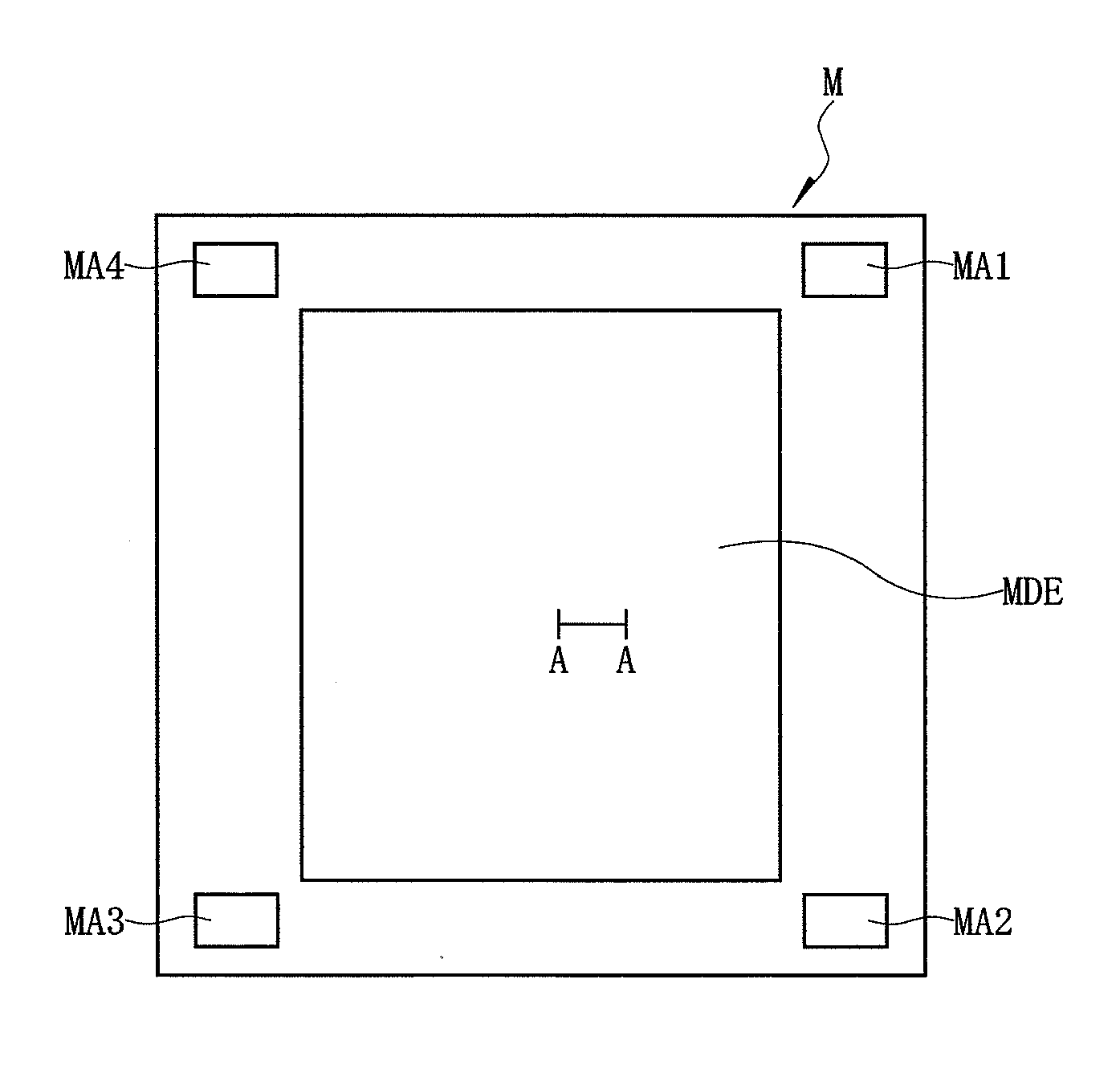
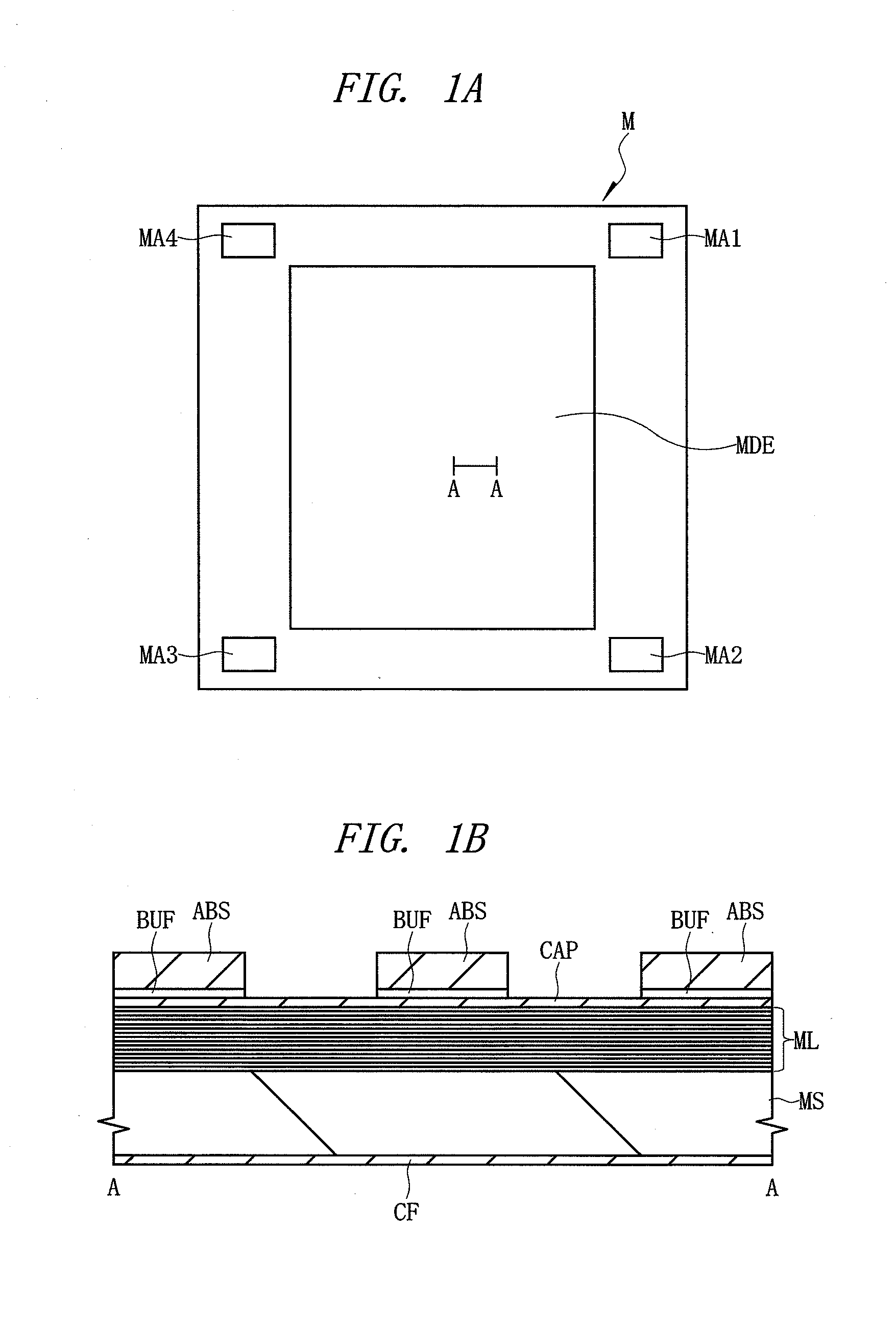
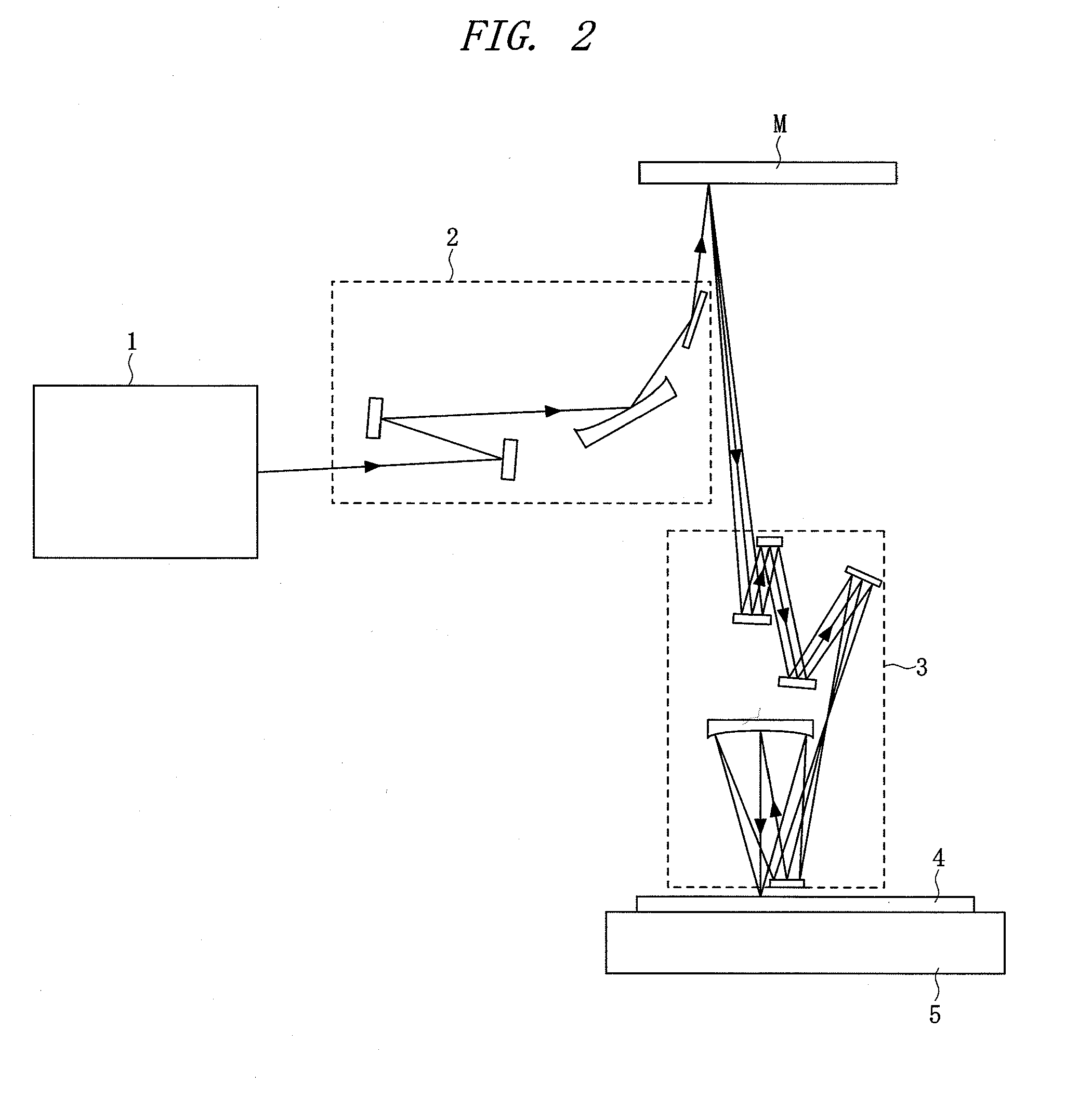
[0051]In order to clarify a purpose of a method of inspecting an EUVL mask according to a first embodiment, first, a structure of the EUVL mask and a structure of a projection optical system (a reduced projection optical system, a reflection-type exposure optical system, a reflection-type imaging optical system, and an EUV optical system) equipped in an EUVL exposure device will be explained with reference to FIGS. 1A, 1B, and 2. FIG. 1A is a plan view of a principal part of a plane on which an absorber pattern of the EUVL mask is formed, and FIG. 1B is a cross-sectional view of a principal part illustrating an enlarged part along line A-A of FIG. 1A. Also, FIG. 2 is a schematic diagram of the EUV projection exposure device.

[0052]As illustrated in FIG. 1A, a device pattern area “MDE” having a circuit pattern of a semiconductor integrated circuit device is provided in a center portion of an EUVL mask “M”, and alignment mark areas “MA1”, “MA2”, “MA3”, and “MA4” including a mark for po...

second embodiment

[0101]In a second embodiment, a method of manufacturing the EUVL mask including the step of inspecting the phase defect of the mask blank and the step of inspecting the phase defect remaining in the EUVL mask explained in the above-described first embodiment will be explained, and the method is capable of apparently reducing or eliminating the influence of the phase defect by adjusting a shape of the absorber pattern in the periphery of the phase defect when it is determined that the remaining phase defect affects the transfer of the absorber pattern.

[0102]First, a mask blank MB is prepared. FIG. 10 is a diagram illustrating one example of the phase defect on the mask blank MB detected by the defect inspection for the mask blank which has been explained in the above-described first embodiment. The phase defects 46-1, 46-2, 46-3, and 46-4 are defects critically affecting when the absorber pattern formed on the mask blank MB is transferred on the main plane of the wafer by the project...


PUM


Abstract

There is provided a method of high-sensitively detecting both of a phase defect existing in a mask blank and a phase defect remaining after manufacturing an EUVL mask. When the mask blank is inspected, EUV light having illumination NA to be within an inner NA but a larger value is irradiated. When the EUVL mask is inspected, by using a dark-field imaging optical system including a center shielding portion for shielding EUV light and a linear shielding portion for shielding the EUV light whose width is smaller than a diameter of the center shielding portion, the center shielding portion and the linear shielding portion being included in a pupil plane, the EUV light having illumination NA as large as or smaller than the width of the linear shielding portion is irradiated.

Description

CROSS-REFERENCE TO RELATED APPLICATION[0001]The present application claims priority from Japanese Patent Application No. 2011-156288 filed on Jul. 15, 2011, the content of which is hereby incorporated by reference into this application.TECHNICAL FIELD OF THE INVENTION[0002]The present invention relates to a technique of manufacturing a lithography mask used for forming a circuit pattern of a semiconductor device. More particularly, the present invention relates to a technique effectively applied to a method of inspecting a mask for extreme ultra-violet ray exposure, a mask inspection device, and a method of manufacturing the mask, the mask being used for a lithography process using so-called extreme ultra-violet ray (EUV light) exposure whose wavelength is about 10 to 15 nm.BACKGROUND OF THE INVENTION[0003]A semiconductor device (semiconductor integrated circuit device) is produced by repeatedly using photolithography in which exposure light is irradiated onto a mask of an original ...

Claims


Application Information

Patent Timeline
IPC IPC(8): G03F1/22G01N21/95
CPCG01N21/8806G01N21/956G03F1/84G01N2021/95676G01N2021/8822G01N21/95G01N2201/061G03F1/22
Inventor TERASAWA, TSUNEOSUGA, OSAMU
Owner RENESAS ELECTRONICS CORP
Why Eureka
Try Eureka