Power semiconductor device

a technology of semiconductor devices and semiconductors, applied in the direction of semiconductor devices, basic electric elements, electrical apparatus, etc., can solve the problems of low cell packing density, low pin effect, and high on-state loss of devices due to a plurality of effects,

Active Publication Date: 2013-01-31
HITACHI ENERGY SWITZERLAND AG
View PDF6 Cites 12 Cited by
  • Summary
  • Abstract
  • Description
  • Claims
  • Application Information

AI Technical Summary

Benefits of technology

[0014]A power semiconductor, is disclosed comprising, a drift layer of a first conductivity type arranged between an emitter electrode on an emitter side and a collector electrode on a collector side of the device; a first base layer of a second conductivity type arranged between the drift layer and the emitter electrode, which first base layer is in direct electrical contact to the emitter electrode; a first source region of the first conductivity type arranged at the emitter side embedded into the first base layer in contact with the emitter electrode, which first source region has a higher doping concentration than the drift layer; a plurality of first gate electrodes, each electrically insulated from the first base layer, the first source region and the drift layer by a first insulating layer, which first gate electrode is arranged in a same plane and lateral to the first base layer and extends deeper into the drift layer than the first base layer, a channel being formable between the emitter electrode, the

Problems solved by technology

The device can have high on-state losses due to a plurality of effects.
Furthermore, due to the lateral channel design, the planar design can incur hole drain effect (PNP effect) due to the bad electron spreading out of the MOS channel.
This PiN effect, however, can only show a positive impact in high voltage devices with low cell packing densities (a low number of cells in an area).
In order to achieve reduced channel resistance the planar devices are made with less cell packing density, and this can only be compensated with narrow pitches (distance between two cells), thereby reducing the PiN effect.
The trench desig

Method used


Image

  • Power semiconductor device
  • Power semiconductor device
  • Power semiconductor device

Examples


Embodiment Construction

[0029]A power semiconductor device is disclosed which can provide on-state losses, improved blocking capability, low drainage of holes and good controllability.

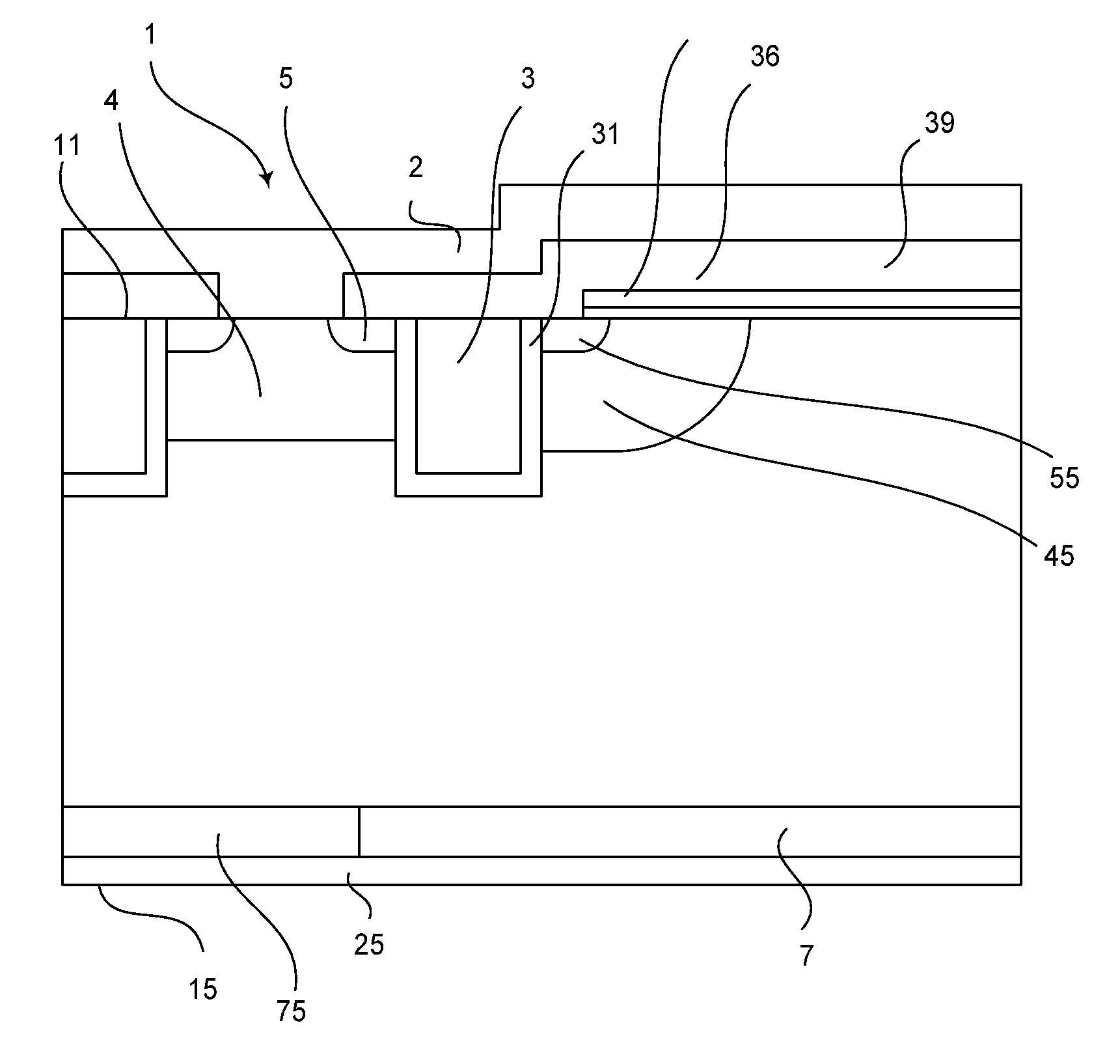
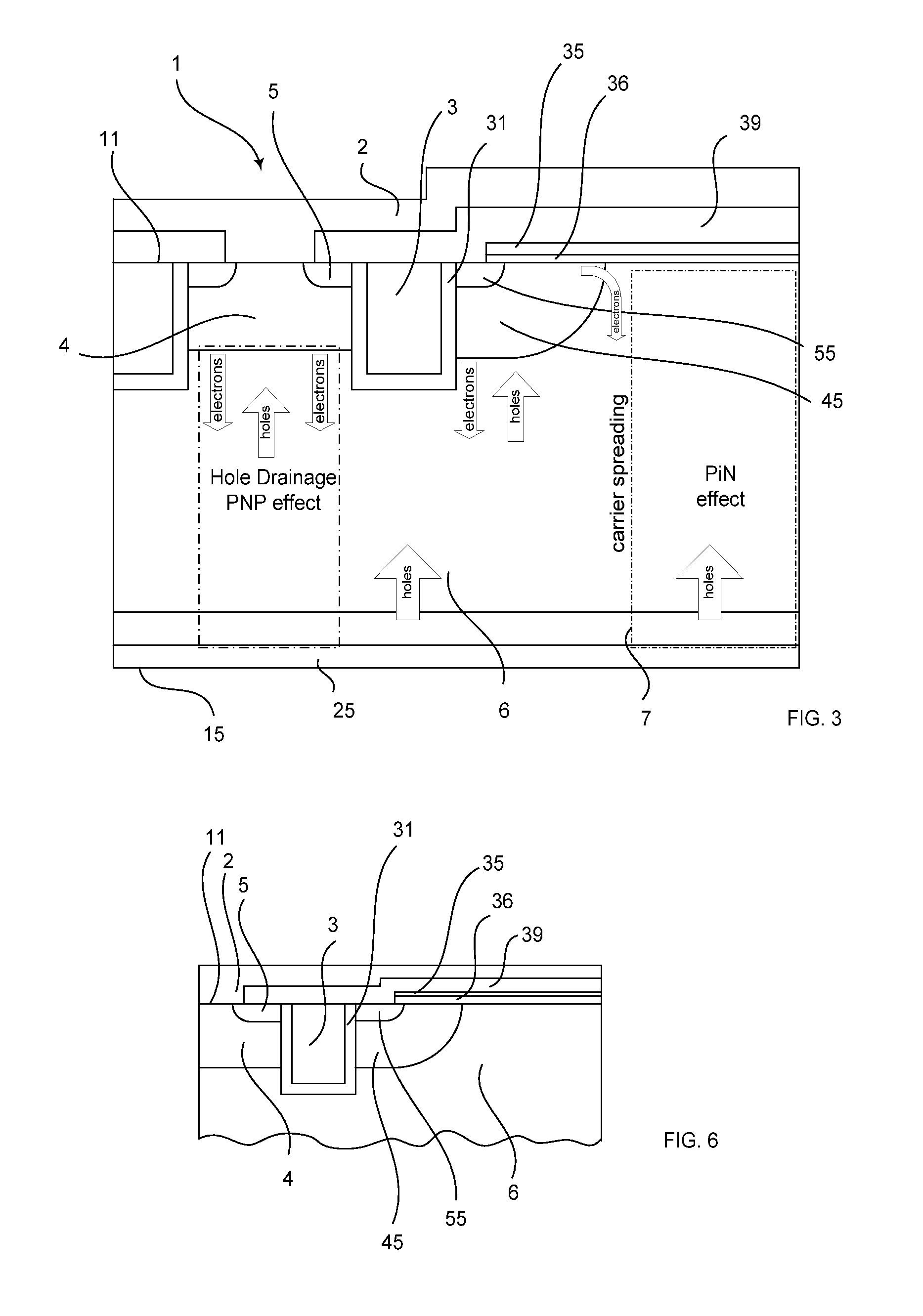
[0030]An exemplary power semiconductor device as disclosed herein has layers of different conductivity types, which layers are arranged between an emitter electrode on an emitter side and a collector electrode on a collector side, which is arranged opposite of the emitter side. The layers can comprise:[0031]a drift layer of a first conductivity type, which is arranged between the emitter side and the collector side,[0032]a first base layer of a second conductivity type, which is arranged between the drift layer and the emitter electrode, which first base layer is in direct electrical contact to the emitter electrode,[0033]a first source region of the first conductivity type, which is arranged at the emitter side embedded into the first base layer and contacts the emitter electrode, which first source region has a higher dopin...


PUM


Abstract

A power semiconductor device is disclosed with layers of different conductivity types between an emitter electrode on an emitter side and a collector electrode on a collector side. The device can include a drift layer, a first base layer in direct electrical contact to the emitter electrode, a first source region embedded into the first base layer which contacts the emitter electrode and has a higher doping concentration than the drift layer, a first gate electrode in a same plane and lateral to the first base layer, a second base layer in the same plane and lateral to the first base layer, a second gate electrode on top of the emitter side, and a second source region electrically insulated from the second base layer, the second source region and the drift layer by a second insulating layer.

Description

RELATED APPLICATION[0001]This application claims priority as a continuation-in-part application under 35 U.S.C. §120 to PCT / EP2011 / 054423, which was filed as an International Application on Mar. 23, 2011 designating the U.S., and which claims priority to European Application 10157392.1 filed in Europe on Mar. 23, 2010. The entire contents of these applications are hereby incorporated by reference in their entireties.FIELD[0002]The present disclosure relates to the field of power semiconductor devices, such as a power semiconductor device with layers of different conductivity types.BACKGROUND INFORMATION[0003]FIG. 1 shows a known IGBT with planar gate electrodes. The IGBT is a device with a four-layer structure, which are arranged between an emitter electrode 2 on an emitter side 11 and a collector electrode 25 on a collector side 15, which is arranged opposite of the emitter side 11. An (n-) doped drift layer 6 is arranged between the emitter side 11 and the collector side 15. A p d...

Claims


Application Information

Patent Timeline
IPC IPC(8): H01L29/739
CPCH01L29/4232H01L29/7397H01L29/7395
Inventor RAHIMO, MUNAFKOPTA, ARNOSTVON ARX, CHRISTOPHANDENNA, MAXI
Owner HITACHI ENERGY SWITZERLAND AG
Why Eureka
Try Eureka