

Damage reduction method and apparatus for destructive testing of power semiconductors
a technology of destructive testing and power semiconductors, which is applied in the direction of short-circuit testing, instruments, measurement devices, etc., can solve the problems of not all chips on the wafer will meet the desired specifications of chips, difficult to use conventional manufacturing processes, and considerable physical damage to semiconductor chips and nearby chips, so as to and limit the damage to the device
- Summary
- Abstract
- Description
- Claims
- Application Information
AI Technical Summary
Benefits of technology
Problems solved by technology
Method used
Image

Examples
Embodiment Construction
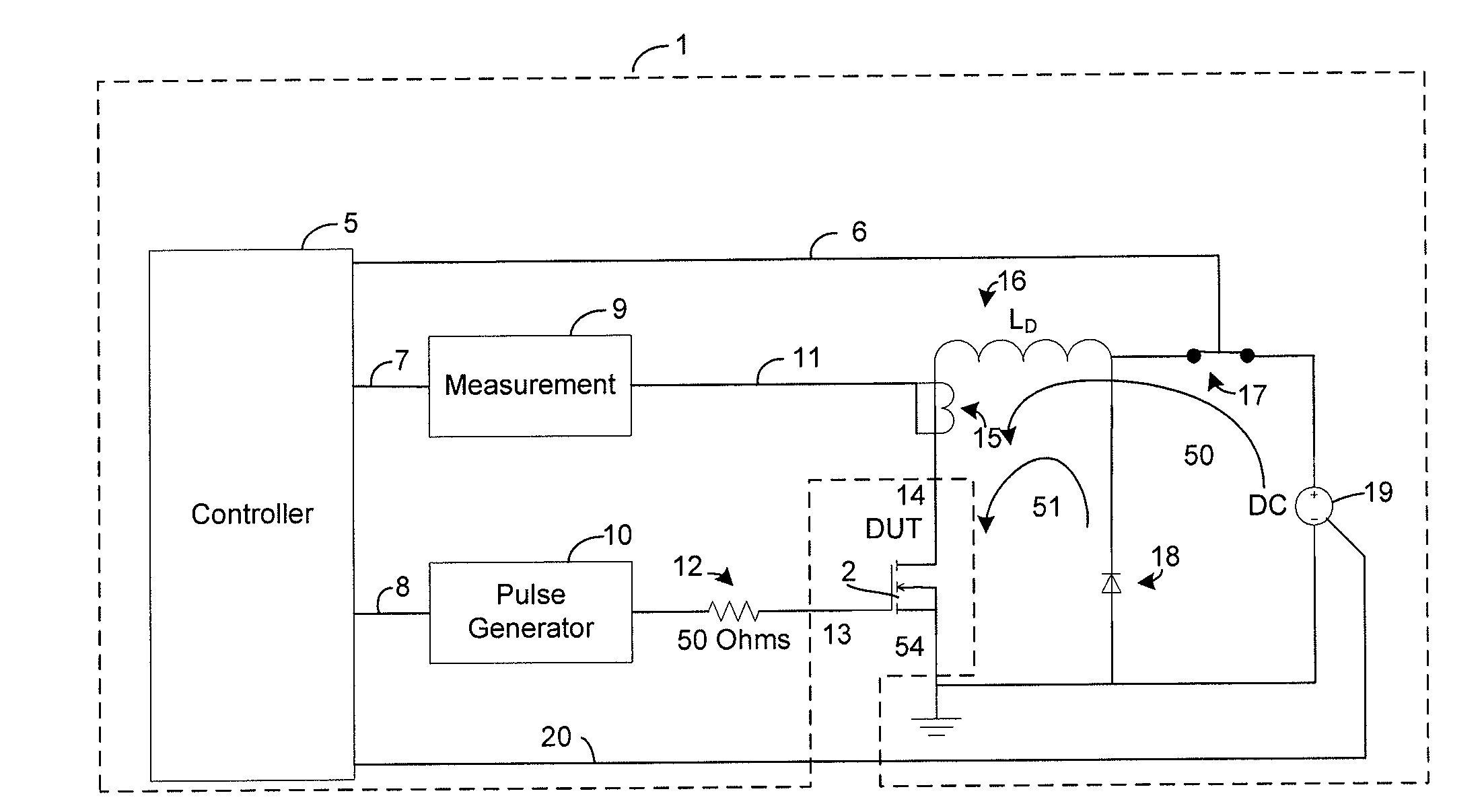
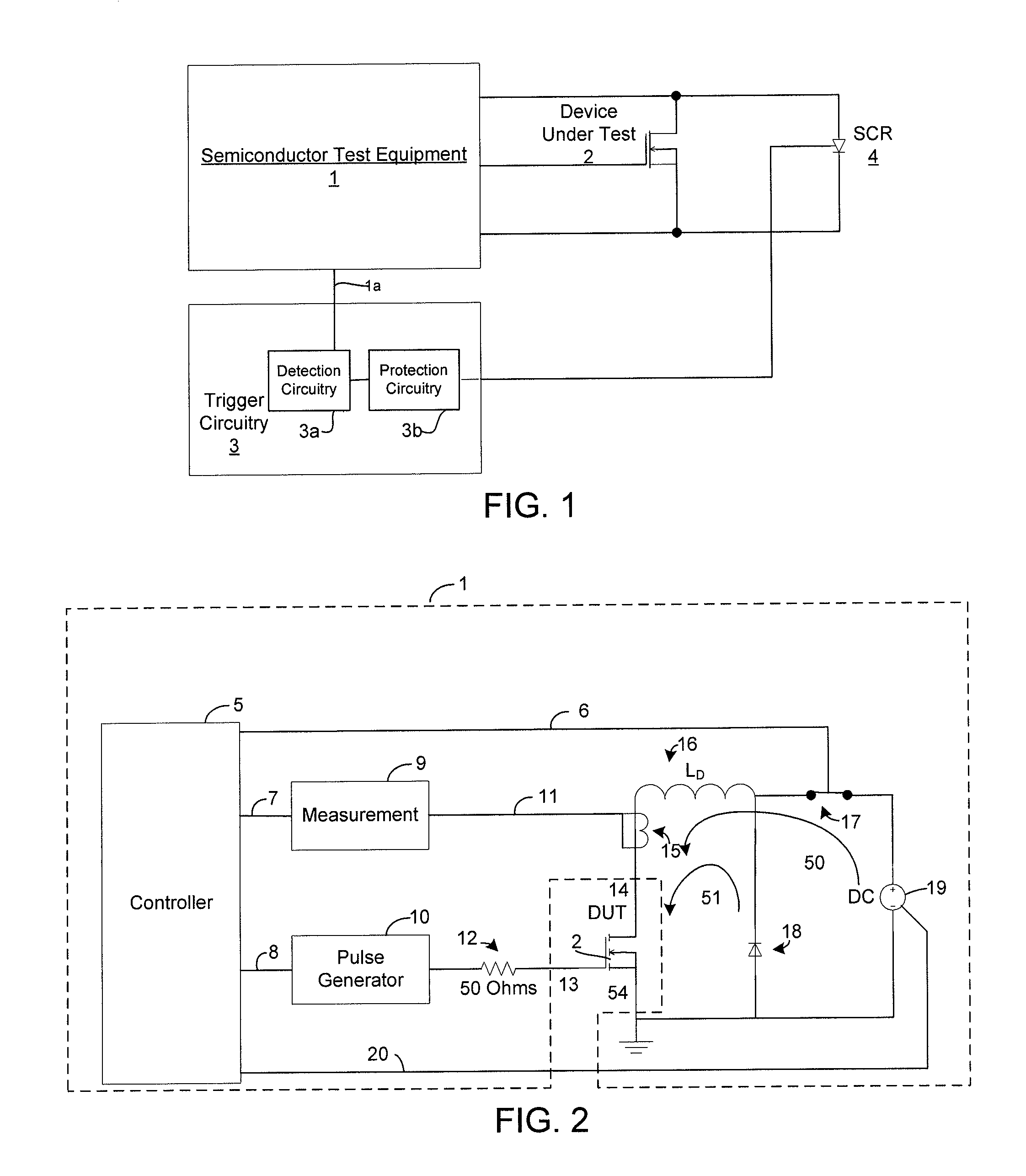
[0038]Referring to FIG. 1, semiconductor test equipment 1, such as an ITC55100 Unclamped Inductive Switching test system, is used to test a device under test 2. It should be appreciated that reference to the ITC55100 test system is merely exemplary, and other semiconductor test systems can be used as the semiconductor test equipment 1 without departing from the scope of the invention. The semiconductor test equipment 1 can perform standard Unclamped Inductive Switching test on devices such as power MOSFET transistors. Thus, in the exemplary configuration shown in FIG. 1, the source, drain and gate connections of the power MOSFET (i.e., the DUT 2 in the present example) are electrically coupled to the semiconductor test equipment 1.
[0039]Additionally, a protective element 4 (e.g., a “crowbar”) such as an SCR, is electrically coupled to the DUT 2 in a parallel configuration. More specifically, an anode and cathode of an SCR 4 are electrically coupled to the DUT 2 (e.g., to the is sour...
PUM
 Abstract
Description
Claims
Application Information