Nonvolatile memory device having a current limiting element

a current limitation and nonvolatile memory technology, applied in semiconductor devices, digital storage, instruments, etc., can solve the problems of difficult to use a low resistance metal oxide film to form the resistance of these films and/or the ratio of high-to-low resistance states is often insufficient to meet the needs of traditional nonvolatile memory technology, and the difficulty of forming a reliable nonvolatile memory device. , to achieve the effect of reducing th

Active Publication Date: 2013-01-31
INTERMOLECULAR
View PDF7 Cites 46 Cited by
  • Summary
  • Abstract
  • Description
  • Claims
  • Application Information

AI Technical Summary

Benefits of technology

[0013]Embodiments of the invention generally relate to a resistive switching nonvolatile memory device having an interface layer structure disposed between at least one of the electrodes and a variable resistance layer formed in the nonvolatile memory device. The resistive switching memory elements may be formed as part of a high-capacity nonvolatile memory integrated circuit, which can be used in various electronic devices, such as digital cameras, mobil...

Problems solved by technology

However, as device dimensions shrink, scaling issues are posing challenges for traditional nonvolatile memory technology.
Although metal oxide (MO) films such as these exhibit bistability, the resistance of these films and/or the ratio of the high-to-low resistance states is (are) often insufficient to be of use within a practical nonvolatile memory device.
Since the variation in the difference in the resistive states is related to the resistance of the resistive switching layer, it is often hard to use a low resistance metal oxide film to form a reliable nonvolatile memory device.
For example, in a nonvolatile memory that has conductive lines formed of a relatively high resistance metal such as tungsten, the resistance of the conductive lines may overwhelm the resistance of the metal oxide resistive switching element if its resistance was not sufficiently high.
This may make it difficult or impossible to sense the state of the bistable metal oxide resistive switching element.
Similar issues can arise from integrati...

Method used


Image

  • Nonvolatile memory device having a current limiting element
  • Nonvolatile memory device having a current limiting element
  • Nonvolatile memory device having a current limiting element

Examples


Embodiment Construction

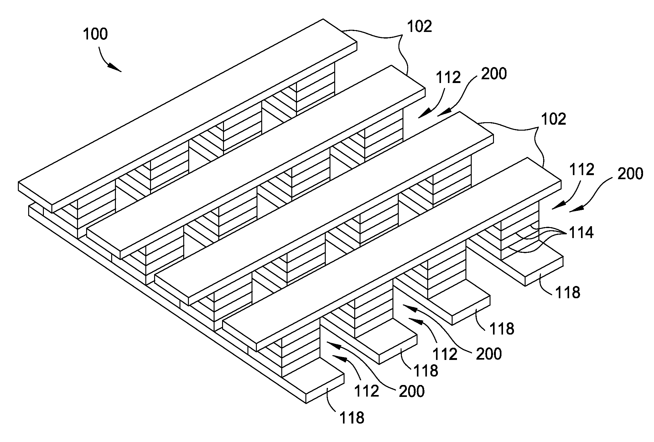
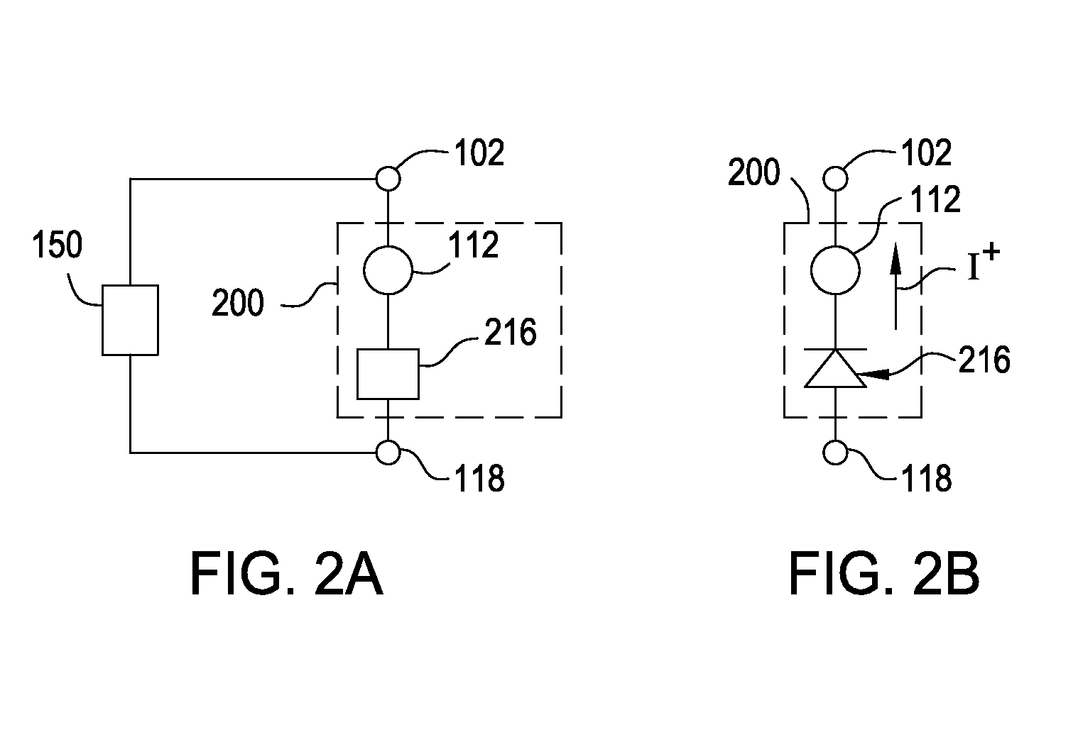
[0031]Embodiments of the invention generally include a method of forming a nonvolatile memory device that contains a resistive switching memory element that has an improved device switching performance and increased usable lifetime, due to the addition of a current limiting component disposed therein. In one embodiment, the current limiting component comprises at least one layer of a resistive material that is disposed within a formed resistive switching memory element in a nonvolatile resistive switching memory device. The electrical properties of the formed current limiting layer, or resistive layer, are configured to lower the current flow through the variable resistance layer by adding a fixed series resistance in the formed nonvolatile resistive switching memory device. It is generally desirable to form the resistive layer so that its material and electrical properties will not degrade or breakdown during the often high current “burn-in” type device preparation steps, such as t...


PUM


Abstract

Embodiments of the invention generally include a method of forming a nonvolatile memory device that contains a resistive switching memory element that has an improved device switching performance and lifetime, due to the addition of a current limiting component disposed therein. In one embodiment, the current limiting component comprises at least one layer of resistive material that is configured to improve the switching performance and lifetime of the formed resistive switching memory element. The electrical properties of the formed current limiting layer, or resistive layer, are configured to lower the current flow through the variable resistance layer during the logic state programming steps (i.e., “set” and “reset” steps) by adding a fixed series resistance in the formed resistive switching memory element found in the nonvolatile memory device.

Description

CROSS-REFERENCE TO RELATED APPLICATIONS[0001]This application claims benefit of U.S. provisional patent application Ser. No. 61 / 513,355, entitled “Nonvolatile Memory Device Having A Current Limiting Element,” filed Jul. 29, 2011, which is herein incorporated by reference.BACKGROUND OF THE INVENTION[0002]1. Field of the Invention[0003]This invention relates to nonvolatile memory elements, and more particularly, to methods for forming resistive switching memory elements used in nonvolatile memory devices.[0004]2. Description of the Related Art[0005]Nonvolatile memory elements are used in systems in which persistent storage is required. For example, digital cameras use nonvolatile memory cards to store images and digital music players use nonvolatile memory to store audio data. Nonvolatile memory is also used to persistently store data in computer environments.[0006]Nonvolatile memory is often formed using electrically-erasable programmable read only memory (EEPROM) technology. This ty...

Claims


Application Information

Patent Timeline
IPC IPC(8): H01L45/00H01L21/8239G11C11/21
CPCG11C13/0007G11C13/003G11C2213/56G11C2213/76H01L45/08H01L45/1253H01L45/1233H01L45/146H01L45/1616H01L27/2409H01L45/12H10B63/20H10B63/80H10N70/24H10N70/801H10N70/826H10N70/8833H10N70/023H10B63/30H10N70/841H10N70/884H10N70/883
Inventor WANG, YUNHASHIM, IMRANCHIANG, TONY
Owner INTERMOLECULAR
Why Eureka
Try Eureka