Method for polishing silicon wafer and polishing liquid therefor

a technology of silicon wafers and polishing liquids, which is applied in the direction of lapping machines, chemical processes, aqueous dispersions, etc., can solve the problems of new process damage to the surface of silicon wafers, defects caused by micro-scratching on the polished surface, etc., and achieve high polishing rate, reduce the outer circumferential portion of the wafer, and achieve the effect of reducing the rolloff ra

Active Publication Date: 2013-02-07
SUMCO CORP
View PDF8 Cites 32 Cited by
  • Summary
  • Abstract
  • Description
  • Claims
  • Application Information

AI Technical Summary

Benefits of technology

[0030]In accordance with the method for polishing silicon wafers and a polishing liquid for the method of the present invention, it is possible to reduce roll-off of a wafer outer circumferential portion while keeping a high polishing rate, which results in making capable flatness (ROA) control of the wafer outer circumferential portion including roll-off and roll-up. Further, it is possible to reduce generation of process damage and defect generation caused by a process such as micro-scratching caused by an aggregation of abrasive grains.

Problems solved by technology

Meanwhile, new process damage has been brought about to the surface of the silicon wafer by a mechanical action during the polishing.
Further, due to aggregation of the free abrasive grains in the polishing liquid, defects caused by a process such as micro-scratching have occurred on a polished surface of a silicon wafer.

Method used


Image

  • Method for polishing silicon wafer and polishing liquid therefor
  • Method for polishing silicon wafer and polishing liquid therefor
  • Method for polishing silicon wafer and polishing liquid therefor

Examples


example 1

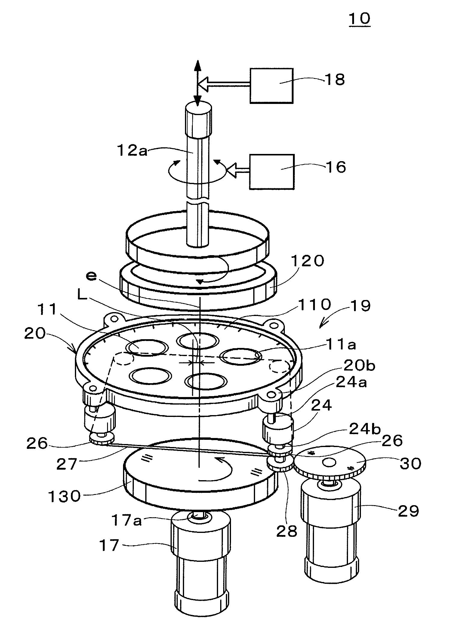
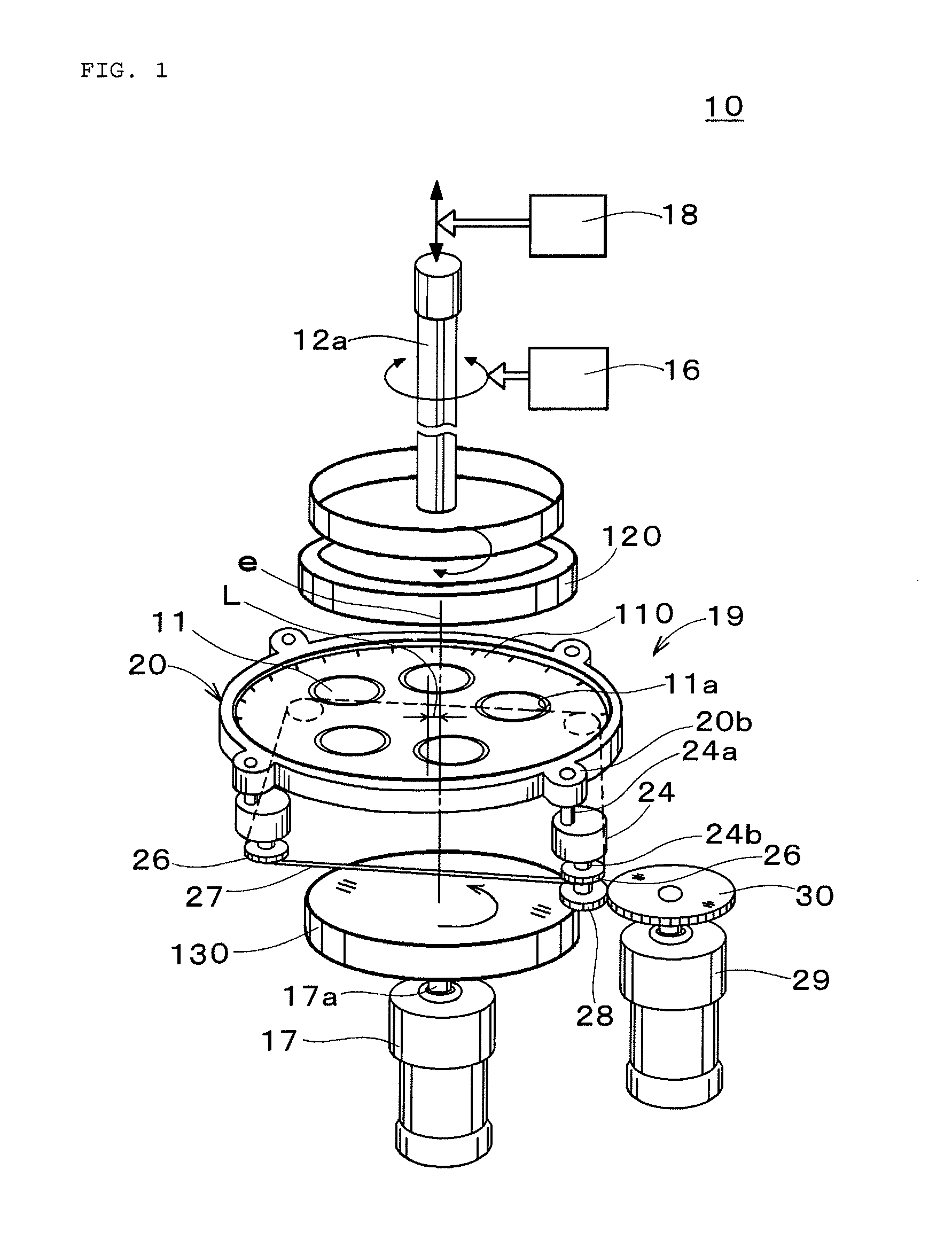
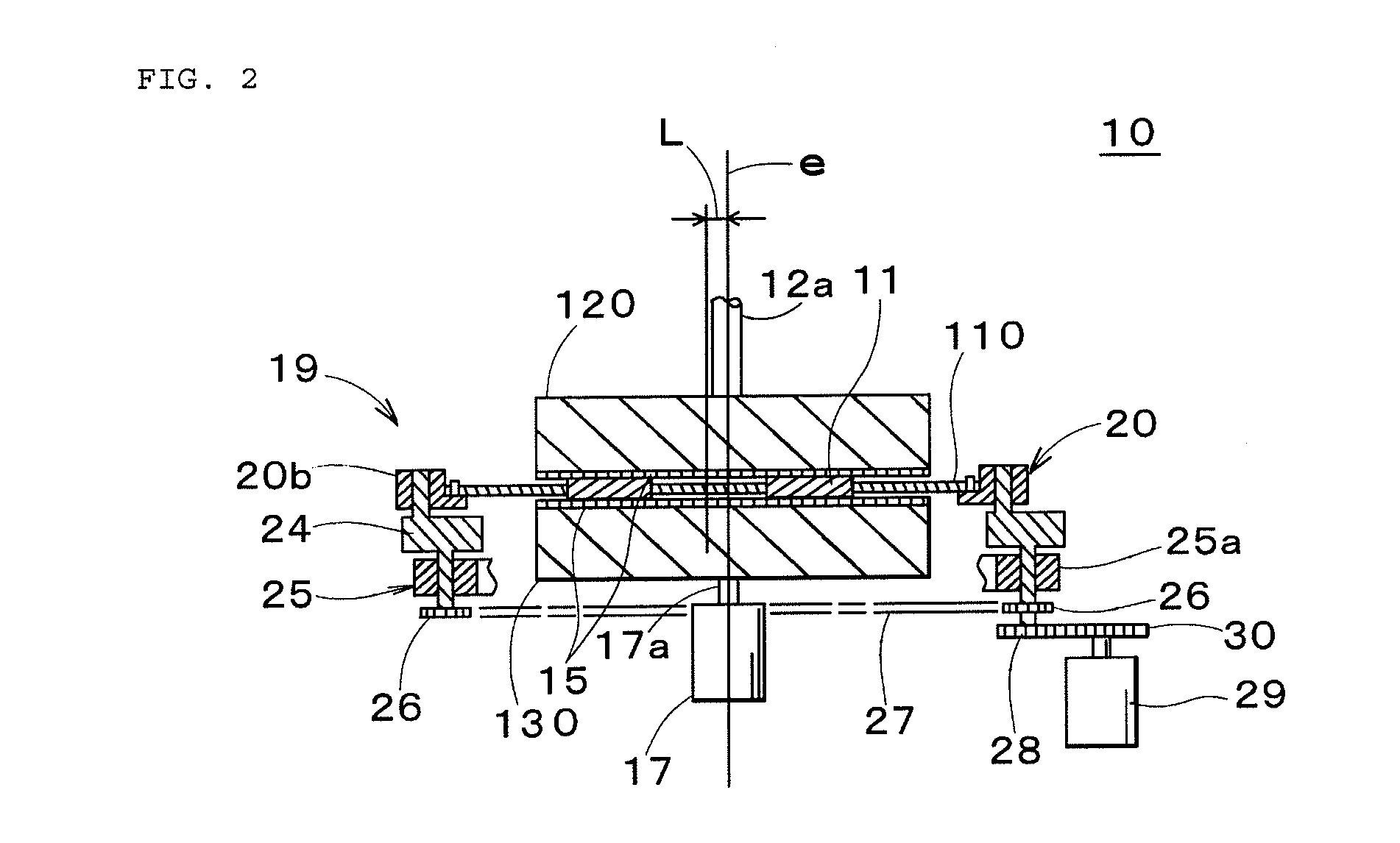
[0084]A method for polishing silicon wafers and a polishing liquid therefor according to Example 1 of the present invention will be described. In Example 1, the rough polishing process is split into two steps to be carried out. As a primary polishing process, the polishing was carried out by use of a polishing liquid containing free abrasive grains in order to eliminate a native oxide film present on the wafer surface, and as a secondary polishing process, the polishing was carried out by use of a polishing liquid with no free abrasive grains in order to achieve flattening of the silicon wafer.

[0085]The double-side polished silicon wafer whose surface and rear surface are mirror-surface polished is manufactured through the following respective processes.

[0086]That is, a monocrystalline silicon ingot with a diameter of 306 mm, a length of its straight body of 2500 mm, a specific resistance of 0.01 Ω·cm, and initial oxygen concentration of 1.0×10¹⁸ atoms / cm3 is pulled up by the Czochr...

example 2

[0110]A method for polishing silicon wafers and a polishing liquid therefor according to Example 2 of the present invention will be described. In Example 2, the secondary polishing process carried out in the present example is further split into two steps (first-step polishing and second-step polishing) to be carried out. The polishing was carried out such that, in the secondary polishing (first-step polishing), the concentration of the water-soluble polymer in the polishing liquid is set to be a low concentration in order to increase the polishing rate of the silicon wafer 11, and in the tertiary polishing (second-step polishing), the concentration of the water-soluble polymer in the polishing liquid is set to be a high concentration in order to inhibit a roll-off amount of the outer circumferential portion of the silicon wafer 11.

[0111]In the invention of Example 2, secondary polishing (first-step polishing) which is the same as the secondary polishing in Example 1 is applied exce...


PUM

PropertyMeasurementUnit
heightaaaaaaaaaa
diameteraaaaaaaaaa
diameteraaaaaaaaaa

Abstract

Disclosed is a method for polishing a silicon wafer, wherein a surface to be polished of a silicon wafer is rough polished, while supplying a polishing liquid, which is obtained by adding a water-soluble polymer to an aqueous alkaline solution that contains no free abrasive grains, to a polishing cloth. Consequently, the surface to be polished can be polished at high polishing rate and the flatness of the edge portion including roll-off and roll-up can be controlled.

Description

TECHNICAL FIELD[0001]This invention relates to a method for polishing silicon wafers and a polishing liquid for the method, and in particular, to a method for polishing silicon wafers for polishing at least the surface serving as a surface to be polished between the surface and the rear surface of the silicon wafer so as to relatively rotate a silicon wafer and an abrasive cloth while supplying a polishing liquid, and the polishing liquid for the method.BACKGROUND ART[0002]In recent years, as a method for polishing a surface of a silicon wafer, CMP (chemical mechanical polishing) which is carried out so as to relatively rotate the silicon wafer and an abrasive cloth while supplying a polishing liquid in which free abrasive grains such as silica grains are contained in an alkaline aqueous solution, is common. CMP has been known by that a mechanical polishing action by free abrasive grains and a chemical polishing action by an alkaline aqueous solution are combined, to be able to obta...

Claims


Application Information

Patent Timeline
Patent Type & Authority Applications(United States)
IPC IPC(8): B24B1/00C09G1/04B24B37/04B24B37/08B24B37/24B24B37/28
CPCB24B37/08B24B37/245B24B37/28B24B37/044H01L21/02024B24B37/04C09K3/14H01L21/304
Inventor OGATA, SHINICHITANIMOTO, RYUICHIYAMASAKI, ICHIROMIKURIYA, SHUNSUKE
Owner SUMCO CORP
Why Eureka
Try Eureka