Capacitive-coupled plasma processing apparatus and method for processing substrate

a plasma processing and coupling technology, applied in the field of plasma processing apparatus and method for processing substrate, can solve the problems of uniformity of the electric field distribution in the reaction chamber of the prior art, and the whole radio frequency electric field in the reaction chamber b>100/b> to be non-uniform, so as to achieve the effect of adjusting the electric field strength, reducing resistance, and increasing the electric field strength

Active Publication Date: 2013-02-07
ADVANCED MICRO FAB EQUIP INC CHINA
View PDF11 Cites 155 Cited by
  • Summary
  • Abstract
  • Description
  • Claims
  • Application Information

AI Technical Summary

Benefits of technology

[0026]Preferably, an induction coil with radio frequency source can be arranged on the electric field regulating element, so as to adjust the electric field strength of the regenerated electric field by adjusting the frequency or the power of the radio frequency source; alternatively, a reluctance regulator with a position regulating means can be further arranged on the electric field regulating element, for moving the reluctance regulator along the axial direction or the radial direction to form a corresponding gap on the electric field regulating element, thereby adjusting the reluctance of the whole magnetic conductive closed loop, so as to adjust the electric field strength of the regenerated electric field. By adjusting the electric field strength of the regenerated electric field, the density distribution of the plasma in the reaction chamber can be further controlled, for example the original situation, in which the plasma density at the central portion of the substrate is higher than that at the edge portion of the substrate, is continuously adjusted to the situation in which the density at the central portion of the substrate and the density at the edge portion of the substrate are substantially uniform, and thus the etching processes performed on various portions of the substrate are more uniform; alternatively, the electric field strength can be further increased or the reluctance can be further decreased, so that the plasma density at the central portion of the substrate is lower than that at the edge portion of the substrate, so as to obtain different processing effects that the etching is slow at the central portion of the substrate and quick at the edge portion of the substrate.
[0027]As a variation of the above several embodiments, it is also possible that the center of the electric field regulating element is deviated from the center of the substrate, thereby obtaining the effect in which the plasma density at the center of the electric field regulating element is lower than that at the edge of the electric field regulating element, which can cooperate with the effect of controlling the plasma density of the radio frequency electric field to obtain different etching effects at different regions of the substrate.

Problems solved by technology

However, the uniformity of the electric field distribution in the reaction chamber of the prior art is far from ideal.
The difference in the actual structures of the two electrodes and the grounded sidewall will lead to bend of the electric field lines, causing the whole radio frequency electric field in the reaction chamber 100 to be non-uniform.

Method used


Image

  • Capacitive-coupled plasma processing apparatus and method for processing substrate
  • Capacitive-coupled plasma processing apparatus and method for processing substrate
  • Capacitive-coupled plasma processing apparatus and method for processing substrate

Examples


embodiment 1

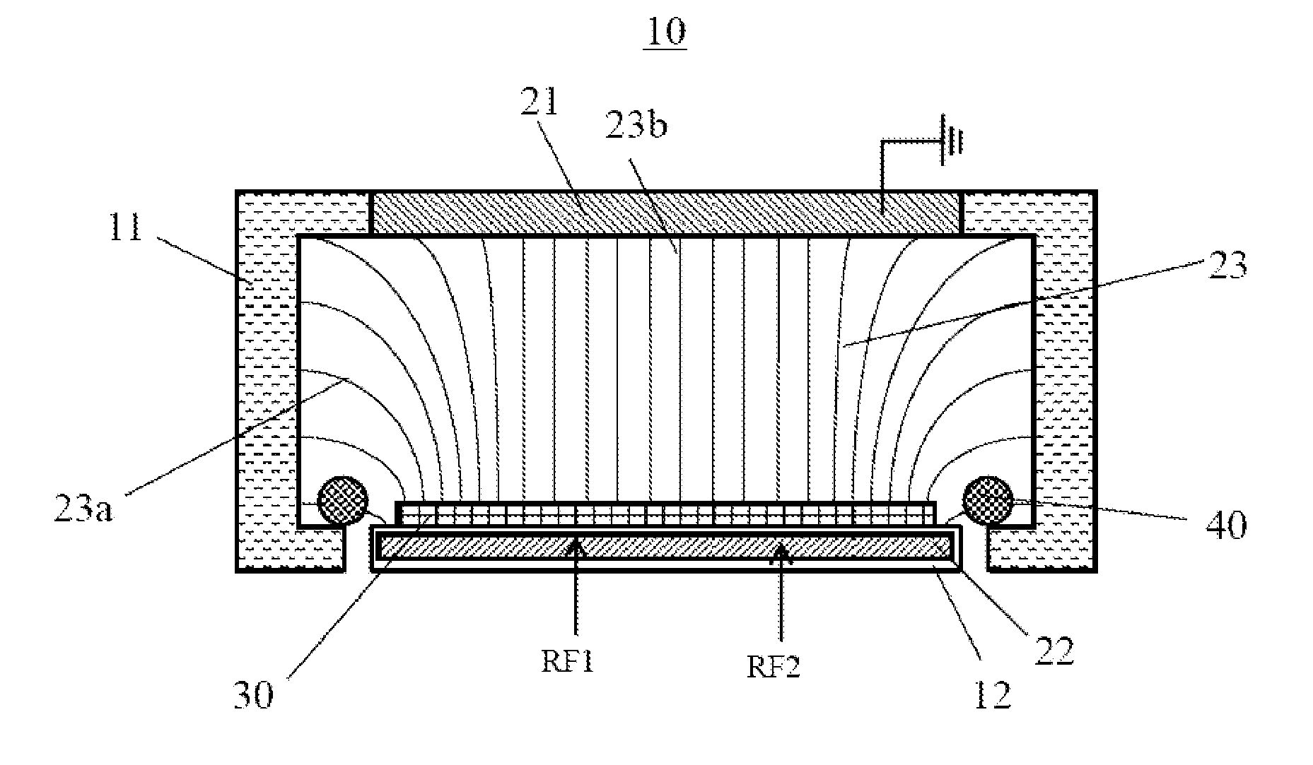
[0038]FIG. 2a is a schematic general structural diagram of a plasma processing apparatus provided by the present invention. The plasma processing apparatus in the diagram is a capacitive-coupled processing apparatus. The capacitive-coupled processing apparatus includes a vacuum reaction chamber 10 into which reaction gas is introduced; a first electrode 21 of planar type is provided in the top portion of the reaction chamber 10, and the first electrode 21 is grounded via the sidewall 11 or is connected to one or more radio frequency power source (not shown); a supporting holder 12 for placing a substrate 30 is provided at the bottom of the reaction chamber 10; and a second electrode 22 of planar type in parallel with the first electrode 21 is provided inside the supporting holder 12. It should be understood that the supporting holder 12 is only exemplary, and the supporting holder 12 can include an electrostatic chuck plate (not shown) and a second electrode 22 under the electrostat...

embodiment 2

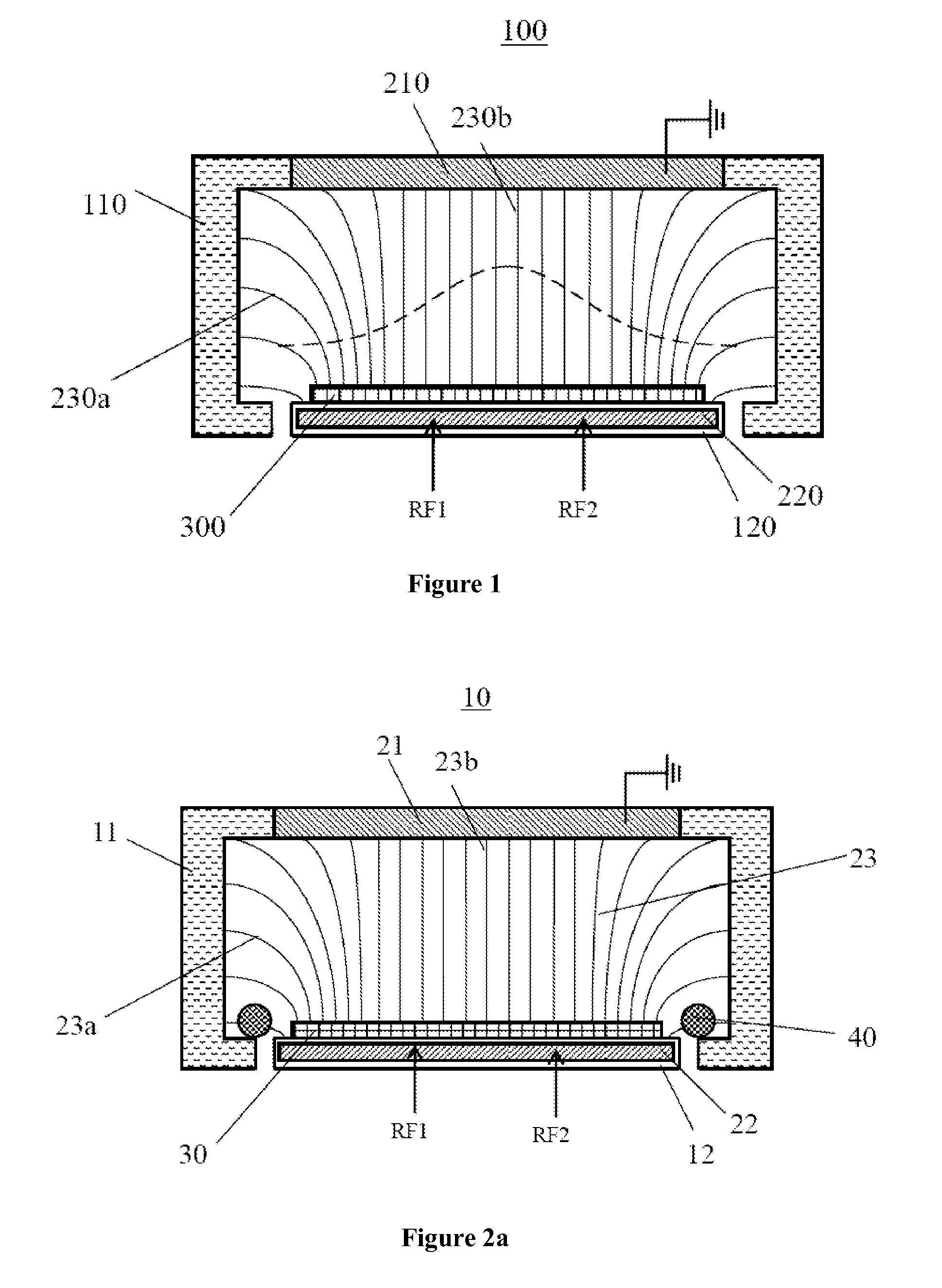
[0045]As shown in FIG. 4, FIGS. 4 is a schematic diagram of another plasma processing apparatus provided by the present invention. Similar to the above embodiment, a second electrode is provided in parallel in the vacuum reaction chamber 102 in which the reaction gas is introduced, and a substrate 30 to be processed is placed on a supporting holder 12 including the second electrode 22. The first electrode 21 is grounded via the sidewall 11 of the reaction chamber 10 or is connected to a radio frequency power source, and at least one radio frequency power source is applied on the second electrode 22, therefore a radio frequency electric field is formed in the reaction chamber 10 to generate plasma of the reaction gas for performing processes such as etching the substrate 30.

[0046]The difference from the above embodiment is that the electric field regulating element 400 in the embodiment shown in FIG. 4 is provided nearby the substrate 30 and is provided inside the sidewall 11 of the ...

embodiment 3

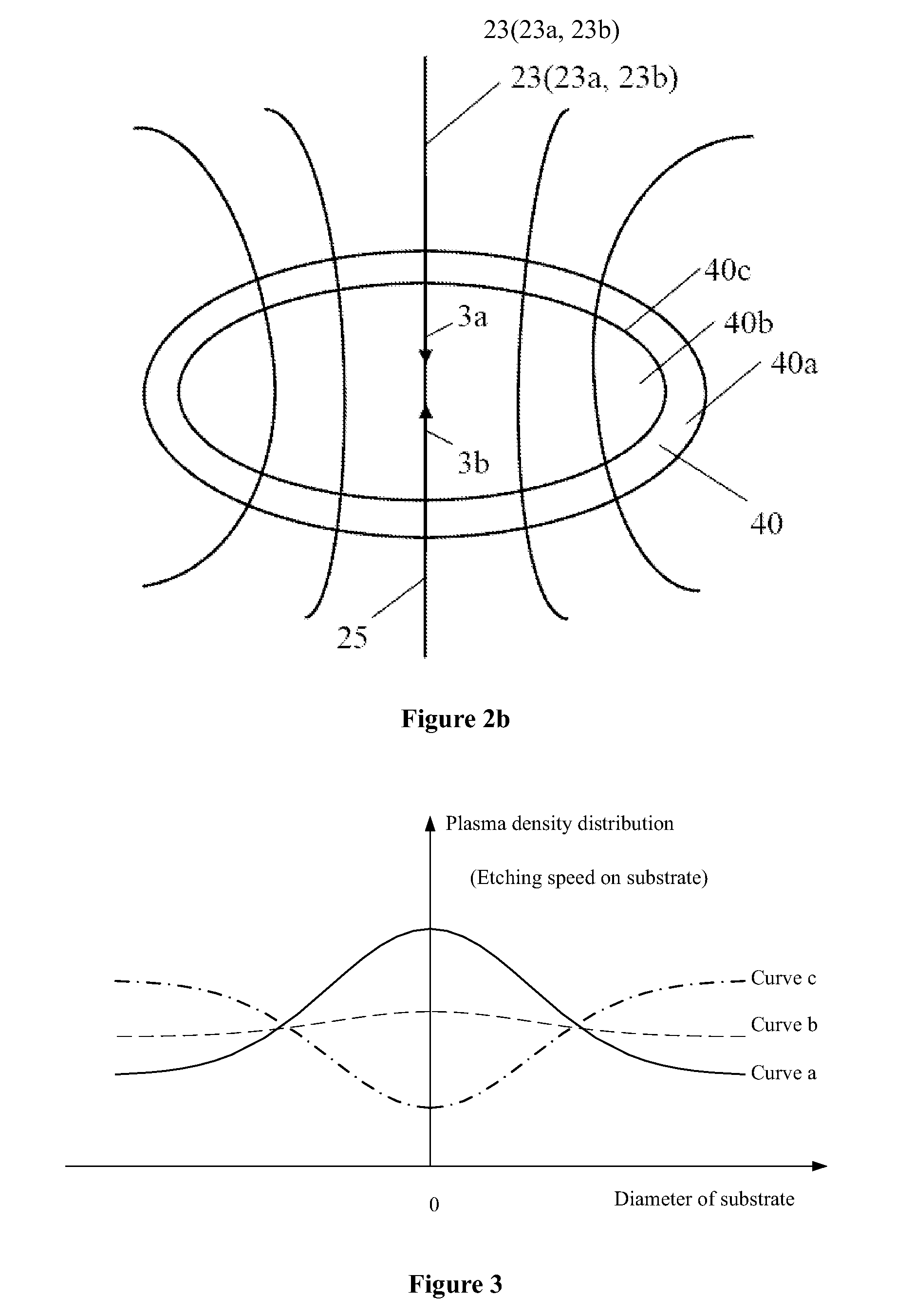
[0048]FIG. 5 is a schematic diagram of the plasma processing apparatus of the present invention, with an active coil being further provided into the first or the second embodiment. As shown in FIG. 5, and referring to FIG. 2a and FIG. 3, the difference from the above embodiments is that at least one induction coil 50 is further provided in this embodiment, which is wound around at least a part of the electric field regulating element 40 / 400. The induction coil 50 can be further connected to an active element or a passive element (denoted by the block 51 in the Figure). For example, as one embodiment, the element 51a is a switching element. When the switching element 51a is closed, the induction coil 50 is shorted. A magnetic field is induced in the electric field regulating element 40 / 400 under the action of the above radio frequency electric field and a new induced current (not shown) on the induction coil 50 is in turn induced by the magnetic field. The new magnetic line generated...


PUM

PropertyMeasurementUnit
frequenciesaaaaaaaaaa
radio frequency electric fieldaaaaaaaaaa
electric fieldaaaaaaaaaa

Abstract

The present invention relates to a capacitive-coupled plasma processing apparatus, wherein an electric field regulating element, i.e., an “electric field lens”, is arranged in the reaction chamber to generate a regenerated electric field in a direction opposite to that of the original radio frequency electric field in the reaction chamber, so that the non-uniformity of etching rate on the surface of the substrate of the plasma incurred by the original radio frequency electric field is decreased; and the electric field regulating element, i.e., the “electric field lens”, further decreases the equivalent quality factor Q value of the reaction chamber, expands the radio frequency band, and prevents high-voltage electric arcing. The present invention further provides a method for processing the substrate using the processing apparatus.

Description

[0001]This application claims the priority of Chinese Patent Application No. 201110219413.5, entitled “CAPACITIVE-COUPLED PLASMA PROCESSING APPARATUS AND METHOD FOR PROCESSING SUBSTRATE”, filed on Aug. 2, 2011 with State Intellectual Property Office of PRC, which is hereby incorporated by reference in its entirety.FIELD OF THE INVENTION[0002]The present invention relates to plasma processing apparatus and method for processing substrate, and in particular to a capacitive-coupled plasma processing apparatus enabling uniform distribution of plasma and a method for processing substrate by using the same.BACKGROUND OF THE INVENTION[0003]At present, in fabricating a semiconductor device, a capacitive-coupled plasma processing apparatus is often adopted to generate plasma of reaction gas for performing processes such as etching and depositing on the substrate.[0004]FIG. 1 shows an existing capacitive-coupled plasma generator, in which at least one pair of planar electrodes, i.e., a first ...

Claims


Application Information

Patent Timeline
Patent Type & Authority Applications(United States)
IPC IPC(8): H05H1/24B44C1/22C23C16/509
CPCH01J37/32091H05H2001/4675H05H1/46H01J37/32669H05H1/466
Inventor LIU, ZHONGDUYIN, GERALD ZHEYAO
Owner ADVANCED MICRO FAB EQUIP INC CHINA
Why Eureka
Try Eureka