Thin film device

a thin film, semiconductor film technology, applied in the direction of semiconductor devices, electrical devices, transistors, etc., can solve the problems of instability of tft characteristics, increase in off-current at the time of irradiation of visible light, and large increase in off-current at the time of irradiation,

Active Publication Date: 2013-02-14
NEC LCD TECH CORP
View PDF13 Cites 10 Cited by
  • Summary
  • Abstract
  • Description
  • Claims
  • Application Information

AI Technical Summary

Problems solved by technology

Further, an increase in the off-current at the time of irradiating visible light is extremely small.
In this Document, it is depicted that a granular surface layer remains on a back channel surface after etching the source / drain electrode constituted with Mo by using CF4 gas plasma and that this may be a cause for the instability of the TFT characteristic.
However, nothing is mentioned therein regarding the surface layer of the etched oxide semiconductor film, and the surface layer is not controlled.
Such etching using the hydrochloric acid leads to an increase in the process cost.
Also, there is an issue that the yield is dramatically decreased due to over-etching of the IGZO film since selective etching of the Ti electrode and the IGZO film is difficult.
As described, there is an issue with the oxide semiconductor TFT that the off-current becomes high since a low-resistance layer due to oxygen depletion tends to be formed on the surface of the oxide semiconductor film.
Thus, how to suppress generation of the oxygen deficit layer is an issue.
Further, when the interface layer existing in the interface between the oxide semiconductor film and the source / drain electrode is individually formed as in the cases of the related techniques described above, the process cost is increased.
Further, the interface layer is of low resistance, so that it is necessary to remove the interface layer in a part where the oxide semiconductor film and the source / drain electrode are not superimposed on one another by performing etching.
Thus, it is difficult to selectively remove only the interface layer by performing etching, so that removal by the etching becomes a cause for deteriorating the yield.
As described above, there is an issue with the oxide semiconductor TFT of the related techniques using the oxide semiconductor film that the off-current becomes high since oxygen depletion is generated in the surface region of the oxide semiconductor film after performing plasma etching of the source / drain electrode.
However, it is a cause for deteriorating the yield and increasing the cost.

Method used


Image

  • Thin film device
  • Thin film device
  • Thin film device

Examples


first exemplary embodiment

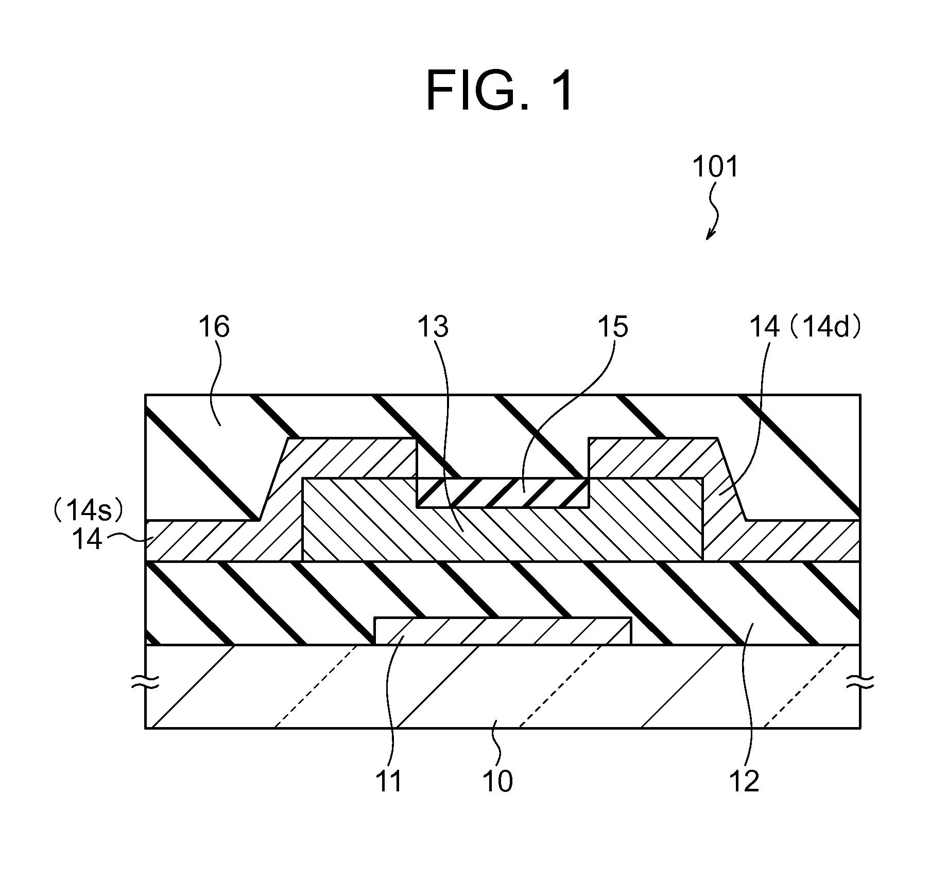
[0029]FIG. 1 is a sectional view showing a channel-etch type TFT 101 according to a first exemplary embodiment. The TFT 101 includes: a gate electrode 11 on an insulating substrate 10 as a substrate; a gate insulating film 12 on the gate electrode 11; an oxide semiconductor film 13 on the gate insulating film 12; and a source / drain electrode 14 on the oxide semiconductor film 13. The TFT 101 is characterized that a surface layer 15 containing at least either fluorine or chlorine exists in a part of the oxide semiconductor film 13 where the source / drain electrodes 14 is not superimposed (e.g., on the oxide semiconductor film 13 between a source electrode 14s and a drain electrode 14d constituting the source / drain electrode 14).

[0030]An example of the manufacturing method of the TFT 101 will be described. First, the gate electrode 11 is formed on the insulating substrate 10, the gate insulating film 12 is formed on the gate electrode 11, and the oxide semiconductor film 13 is formed o...

second exemplary embodiment

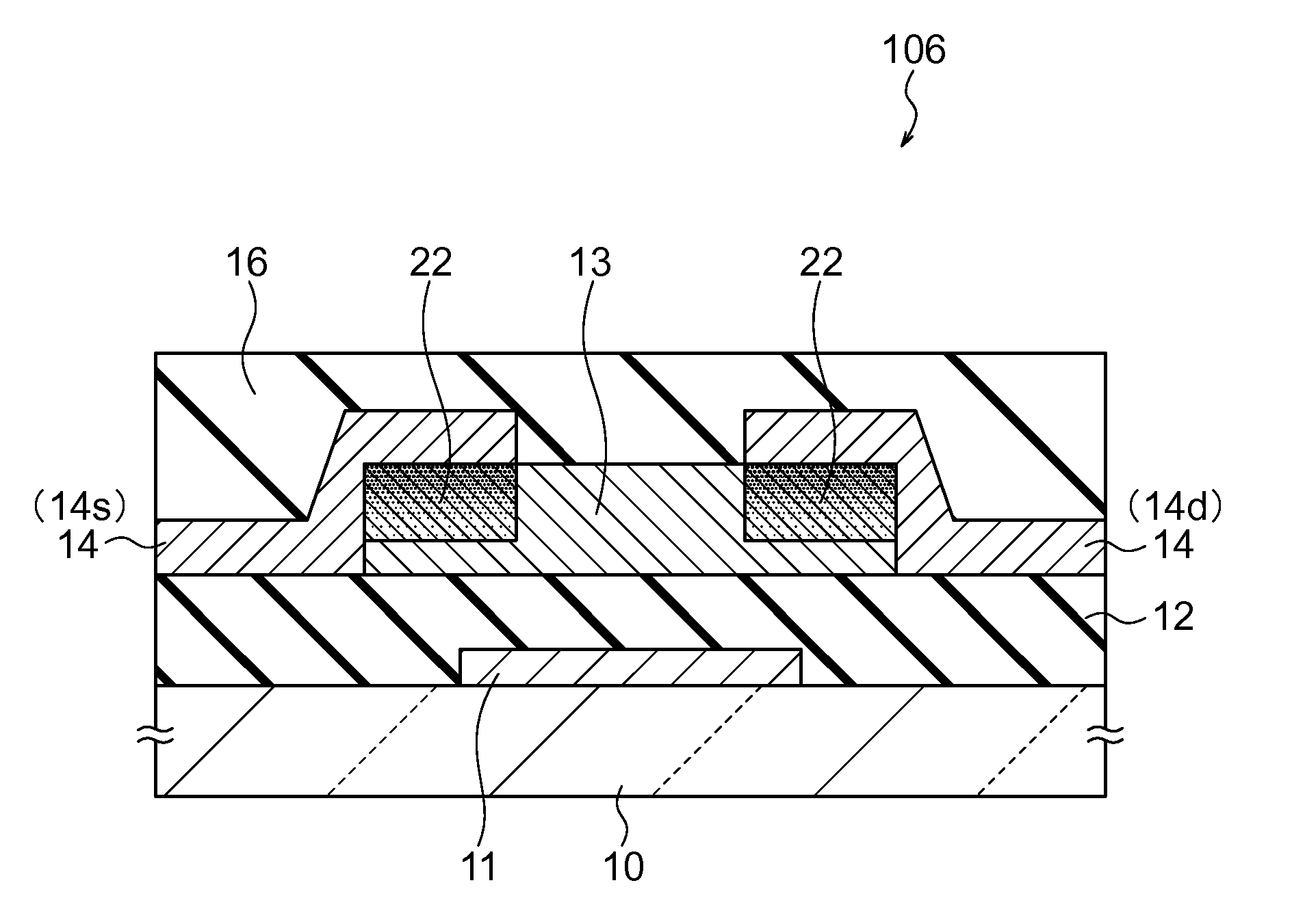
[0043]FIG. 3 is a sectional view showing a channel-etch type TFT 102 according to a second exemplary embodiment. The TFT 102 is characterized to include a compound surface layer 17 as the surface layer containing a composition element of an oxide semiconductor film 13, a composition element of a part of a source / drain electrode 14 to be in contact with the oxide semiconductor film 13, and at least either fluorine or chlorine. Other structures of the TFT of the second exemplary embodiment are the same as the case of the TFT of the first exemplary embodiment.

[0044]An example of the manufacturing method of the TFT 102 will be described. In the second exemplary embodiment, at the time of forming the source / drain electrode 14 on the oxide semiconductor film 13, the compound surface layer 17 containing the composition element of the oxide semiconductor film 13, the composition element of the part of the source / drain electrode 14 to be in contact with the oxide semiconductor film 13, and a...

third exemplary embodiment

[0053]FIG. 5 is a sectional view showing a channel-etch type TFT 103 according to a third exemplary embodiment. In the TFT 103 of the third exemplary embodiment, a mixed layer 18 containing a mixture of a composition element of an oxide semiconductor film 13 and a composition element of a part of a source / drain electrode 14 to be in contact with the oxide semiconductor film 13 exists in the interface between the oxide semiconductor film 13 and the source / drain electrode 14. Further, in the TFT 103, a multiple-element surface layer 19 constituted with the composition elements of the mixed layer 18 and at least either fluorine or chlorine exists as the surface layer. Other structures of the TFT of the third exemplary embodiment are the same as the case of the TFT of the first or second exemplary embodiment.

[0054]An example of the manufacturing method of the TFT 103 will be described. In the third exemplary embodiment, at the time of forming the source / drain electrode 14 on the oxide s...


PUM


Abstract

There is such an issue with a TFT using an oxide semiconductor film that oxygen deficit is generated in a surface region of the oxide semiconductor film after performing plasma etching of a source-drain electrode, and the off-current becomes increased. Disclosed is the TFT which includes: a gate electrode on an insulating substrate as a substrate; a gate insulating film on the gate electrode; an oxide semiconductor film on the gate insulating film; and a source/drain electrode on the oxide semiconductor film. It is the characteristic of the TFT that a surface layer containing at least either fluorine or chlorine exists in a part of the oxide semiconductor film where the source/drain electrode is not superimposed.

Description

CROSS-REFERENCE TO RELATED APPLICATION[0001]This application is based upon and claims the benefit of priority from Japanese patent application No. 2011-177305, filed on Aug. 12, 2011, the disclosure of which is incorporated herein in its entirety by reference.BACKGROUND OF THE INVENTION[0002]1. Field of the Invention[0003]The present invention relates to a thin film device such as an oxide semiconductor thin film transistor which uses an oxide semiconductor film as an active layer. Hereinafter, the thin film transistor is referred to as “TFT”, and an oxide semiconductor composed mainly of indium (In), gallium (Ga), zinc (Zn), and oxygen (O) is referred to as “IGZO (In—Ga—Zn—O)”.[0004]2. Description of the Related Art[0005]Regarding a TFT in which the oxide semiconductor film is used for the active layer, the field-effect mobility is higher than that of a conventional amorphous silicon TFT for about one digit. Further, an increase in the off-current at the time of irradiating visible...

Claims


Application Information

Patent Timeline
Patent Type & Authority Applications(United States)
IPC IPC(8): H01L29/786
CPCH01L29/7869H01L29/78606H01L29/78696
Inventor TAKECHI, KAZUSHIGE
Owner NEC LCD TECH CORP
Why Eureka
Try Eureka