Optical Fibers Functionalized with Photonic Crystal Resonant Optical Structures

a technology of optical fibers and photonic crystals, applied in the field of optical fibers functionalized with photonic crystal resonant optical structures, can solve the problems of difficult integration in large systems with many devices, difficult coupling of light on and off-chip, and no optical fiber has demonstrated functional cavities coupled to the tip of optical fibers, etc., to achieve simple and durable construction, tight space, and easy to mak

Inactive Publication Date: 2013-02-14
THE BOARD OF TRUSTEES OF THE LELAND STANFORD JUNIOR UNIV
View PDF1 Cites 13 Cited by
  • Summary
  • Abstract
  • Description
  • Claims
  • Application Information

AI Technical Summary

Benefits of technology

[0028]PC cavities can be made as small as a fraction of a micron in each dimension which makes them great for near-field sensing and detection. Whereas a typical fiber will be limited by diffraction in its ability to sense features smaller than 5-10 microns in size, PC cavities can strongly localize light in a much tighter space. This means that one can use such devices for monitoring features at the sub-micron level, similar to traditional near-field scanning optical microscopy. These near-field devices are simpler and more durable than conventional near-field probes which are extremely fragile and hard to make (and accordingly very expensive). One can use the fiber plus PC (or fiberPC) device to monitor near-field effects via perturbations in cavity spectral features. These perturbations would allow for the sensing, e.g., of metal-tagged biological samples for cancer detection, as well as differences in the surrounding environment of the fiberPC (such as refractive index).
[0029]The strong intensity of light that is concentrated in PC cavities can be used to locally and resonantly enhance the properties of external samples. Pump light sent from within the fiber can be concentrated at a cavity on the fiber tip which can then resonantly excite particles within the cavity near field. This enhancement can be orders of magnitude more efficient than regular pumping schemes due to near-field effects provided by the cavity. The reverse process is also true, where molecules or nanoparticles can emit more strongly back into the fiber due to the presence of nearby cavities. Both of these effects can be achieved simultaneously (by using a cavity with multiple resonances), and can be used to improve sensitivity to weak emitters that are important for biological studies and cancer detection. Additionally, the resonant enhancement combined with the sub-micron size of the cavity can be advantageous in optogenetics studies. Normally fibers excite large groups of neurons because of diffraction, but here the fiberPC has the size resolution necessary to discriminate and probe single cells.
[0030]PC cavities coupled to fibers can find uses in traditional long-haul fiber optic communications. Depending on the application, photonic crystal cavities can be made into lasers, switches, modulators, and filters. All of these are necessary components in fiber optic communications and are normally made from monolithic chip packages which requires expensive coupling and alignment. Incorporating these components at the tip of a fiber (or even sandwiched between two fibers for an in-line package) could provide drastic improvements in cost and simplicity.
[0031]The fiberPC architecture could also be used in proposed quantum communication systems in the future which use single or entangled photons. A great deal of work has revolved around quantum emitters embedded in PC cavities but so far these experiments are limited to laboratory based testing. Having the quantum emitters directly bound to fiber facets as in the present approach could provide improved practicality of these communications systems.
[0032]Finally, common optics lab components can be simplified and miniaturized with photonic crystal cavities. One example is a cavity-based non-linear frequency converter which could replace conventional non-linear crystals with the advantage of efficient fiber coupling compared to free space optics.

Problems solved by technology

This form factor is convenient for free space optical testing in the laboratory, but is difficult to integrate in larger systems having many devices.
Coupling light on- and off-chip is challenging due to severe size mismatch between PC components and external fiber optics.
Previous studies have shown the transfer of PC cavities onto rigid or flexible substrates, but, to our knowledge, none have demonstrated functional cavities coupled to the tip of an optical fiber.
A micromanipulator stage is used for positioning but we note that the precision required is low since the working fiber facet area is quite large.

Method used


Image

  • Optical Fibers Functionalized with Photonic Crystal Resonant Optical Structures
  • Optical Fibers Functionalized with Photonic Crystal Resonant Optical Structures
  • Optical Fibers Functionalized with Photonic Crystal Resonant Optical Structures

Examples


Embodiment Construction

[0048]In this description, section A provides a description of principles relating to various embodiments of the invention, and section B describes some experimental results.

A) Principles

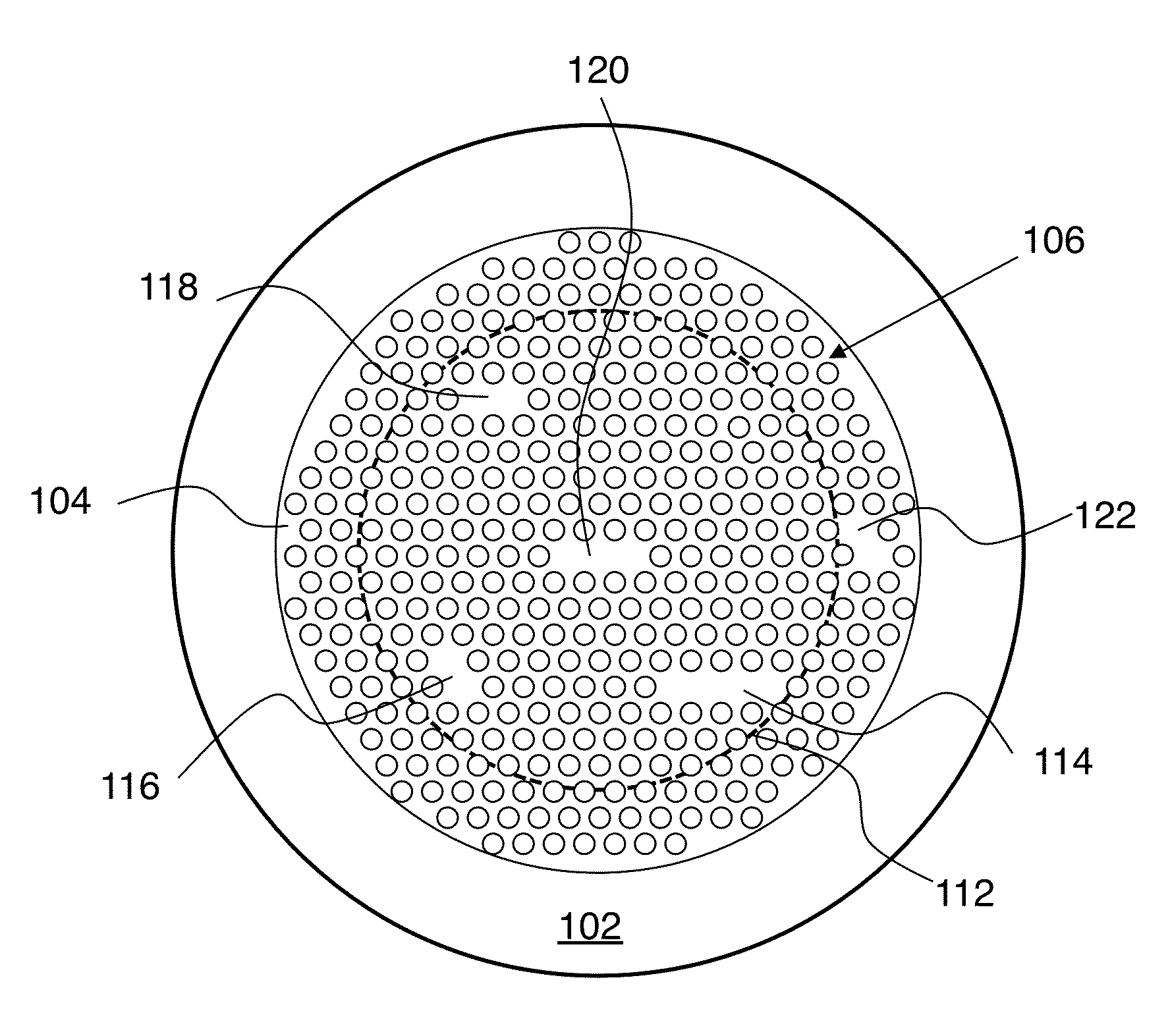
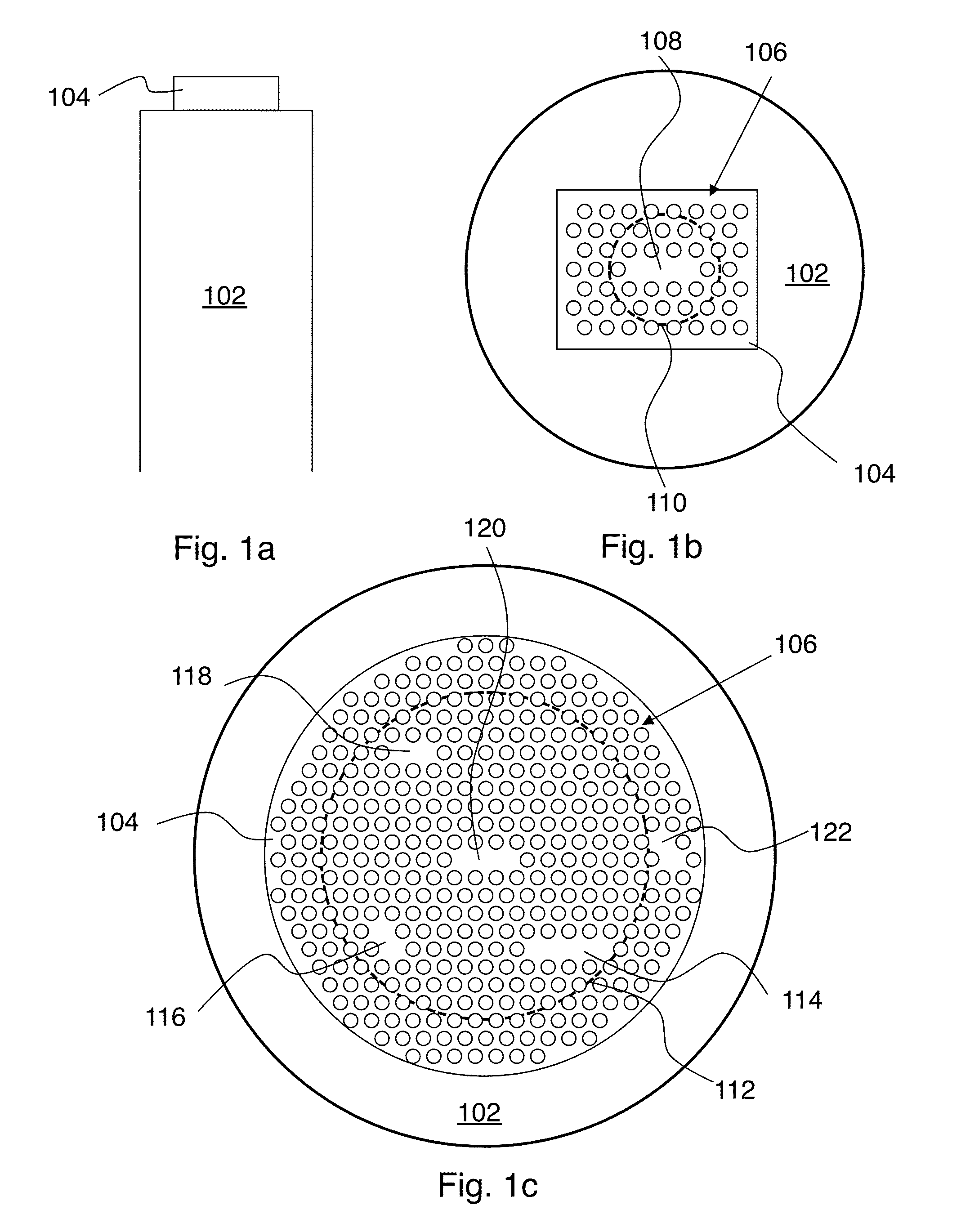
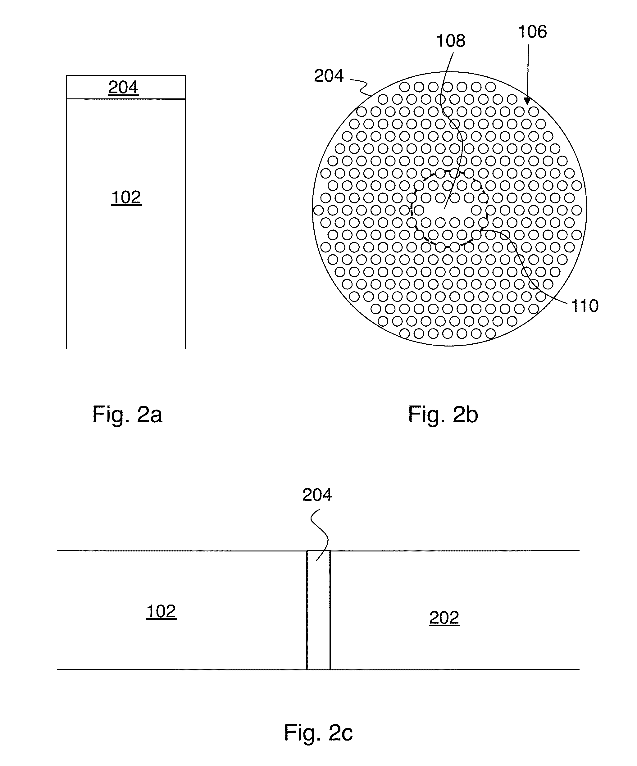
[0049]FIGS. 1a-c show some embodiments of the invention. FIG. 1a shows a side view and FIG. 1b shows a corresponding top view. Here a device 104 is affixed to an exposed end face of optical fiber 102. Device 104 includes at least one resonant optical structure (e.g., cavity 108) defined by a photonic crystal structure 106 in a semiconducting or dielectric material. Fiber 102 is optically coupled to cavity 108 (e.g., by providing a spatial overlap of the fiber core 110 and cavity 108). As described in detail below, device 104 is fabricated on a substrate distinct from fiber 102, and then transferred to fiber 102. FIG. 1c shows a variant. Here fiber core 112 overlaps with several cavities (114, 116, 118, 120), and cavity 122 does not overlap with the core. Instead, cavity 122 is aligned with the cladd...


PUM

PropertyMeasurementUnit
sizeaaaaaaaaaa
thickaaaaaaaaaa
diameteraaaaaaaaaa

Abstract

A photonic crystal (PC) device including one or more resonant optical structures defined by the photonic crystal structure is affixed to the end face of an optical fiber. The PC device is fabricated on a separate substrate, and then affixed to the fiber end face. This transfer can be facilitated by device templates which are laterally supported by tabs after an undercut etch. The tabs can be designed to break during transfer to the fiber, thereby facilitating transfer. Registration marks and/or the use of device templates having the same diameter as the fiber can be used to provide lateral alignment of the fiber to the resonant optical structures. Such alignment may be needed to provide optical coupling between the fiber and the resonant optical structures.

Description

CROSS REFERENCE TO RELATED APPLICATIONS[0001]This application claims the benefit of U.S. provisional patent application 61 / 574,750, filed on Aug. 8, 2011, entitled “Optical Fibers Functionalized with Photonic Crystal Cavities”, and hereby incorporated by reference in its entirety.FIELD OF THE INVENTION[0002]This invention relates to fiber-coupled photonic crystal devices.BACKGROUND[0003]A photonic crystal (PC) has a periodic array of features (e.g., holes) in a background medium. Various devices can be fabricated by modifying the basic structure of a photonic crystal. For example, a PC cavity can be formed by a small cluster of missing holes in a PC lattice (effectively forming a point defect in the PC). As another example, a PC waveguide can be formed by a line of missing holes in a PC lattice.[0004]Photonic crystal devices can readily be fabricated on various semiconducting and / or dielectric substrates. However, it is often difficult to efficiently couple to the resulting PC devic...

Claims


Application Information

Patent Timeline
Patent Type & Authority Applications(United States)
IPC IPC(8): G02B6/12B44C1/22B32B38/10B32B37/12
CPCG02B6/30Y10T156/10B82Y20/00G02B6/1225G02B1/005G02B6/262
Inventor SHAMBAT, GARYVUCKOVIC, JELENA
Owner THE BOARD OF TRUSTEES OF THE LELAND STANFORD JUNIOR UNIV
Why Eureka
Try Eureka