Resonating element, resonator, electronic device, electronic apparatus, and mobile object

a resonator and resonating element technology, applied in the field of res, can solve the problems of reducing the s/n ratio, cracking, or the like, inflicting chipping, cracking or the like on the cut surface, etc., and achieve the effect of satisfactory s/n ratio and excellent frequency stability

Active Publication Date: 2013-02-21
SEIKO EPSON CORP
View PDF9 Cites 29 Cited by
  • Summary
  • Abstract
  • Description
  • Claims
  • Application Information

AI Technical Summary

Benefits of technology

[0055]According to the configuration, since the piezoelectric resonator of the above application example is used in a mobile object, there is an effect of configuring a mobile object having excellent frequency stability at a high frequency and including a reference frequency source with a satisfactory S / N ratio.

Problems solved by technology

However, in JP-A-2002-033640 (patent literature 5), in order to obtain the L-shaped thick section, the thick section is cut out along a line α and a line β as described in FIGS. 1C and 1D of JP-A-2002-033640, but since cutting is performed on the premise of cutting using a mechanical process such as dicing, or the like, there are problems in that damage such as chipping, cracking, or the like is inflicted on a cut surface, and an ultra-thin section is broken.
In addition, other problems occur such as the generation of unwanted vibration that may cause spurious vibrations in a vibration area, an increase of a CI value, or the like.
When miniaturization of a piezoelectric resonator is designed to achieve, there is a case where deterioration in electric characteristics or degradation of a frequency aging characteristic are caused due to residual stress caused by an adhesive.
It is said that the use of such a configuration can hinder residual stress from expanding to a vibration area.
However, when miniaturization and high frequency are intended, it is clear that there is a problem in that, with regard to a piezoelectric resonator of the above-described configuration, a CI value of the main vibration, a ratio of CI values of proximate spurious vibrations (=CIs / CIm, wherein CIm is a CI value of the main vibration, and CIs is a CI value of spurious vibrations, and a standard example is 1.8 or higher) and the like do not satisfy the demands.
Particularly, when a frequency is a high frequency of several hundred MHz, the thickness of an electrode film of an excitation electrode formed in a piezoelectric vibration element and a lead electrode are problematic.
When only the main vibration of the piezoelectric vibration element is intended to be in a trapping mode, there are problems in that the electrode film is thin, ohmic loss arises, and the CI value of the piezoelectric vibrating element increases.
In addition, when the thickness of the electrode film is thickened in order to prevent ohmic loss of the film, there is a problem in that many inharmonic modes other than the main vibration are shifted to trapping modes, and thus, the ratio of CI values of proximate spurious vibrations is not attained.

Method used


Image

  • Resonating element, resonator, electronic device, electronic apparatus, and mobile object
  • Resonating element, resonator, electronic device, electronic apparatus, and mobile object
  • Resonating element, resonator, electronic device, electronic apparatus, and mobile object

Examples


first embodiment

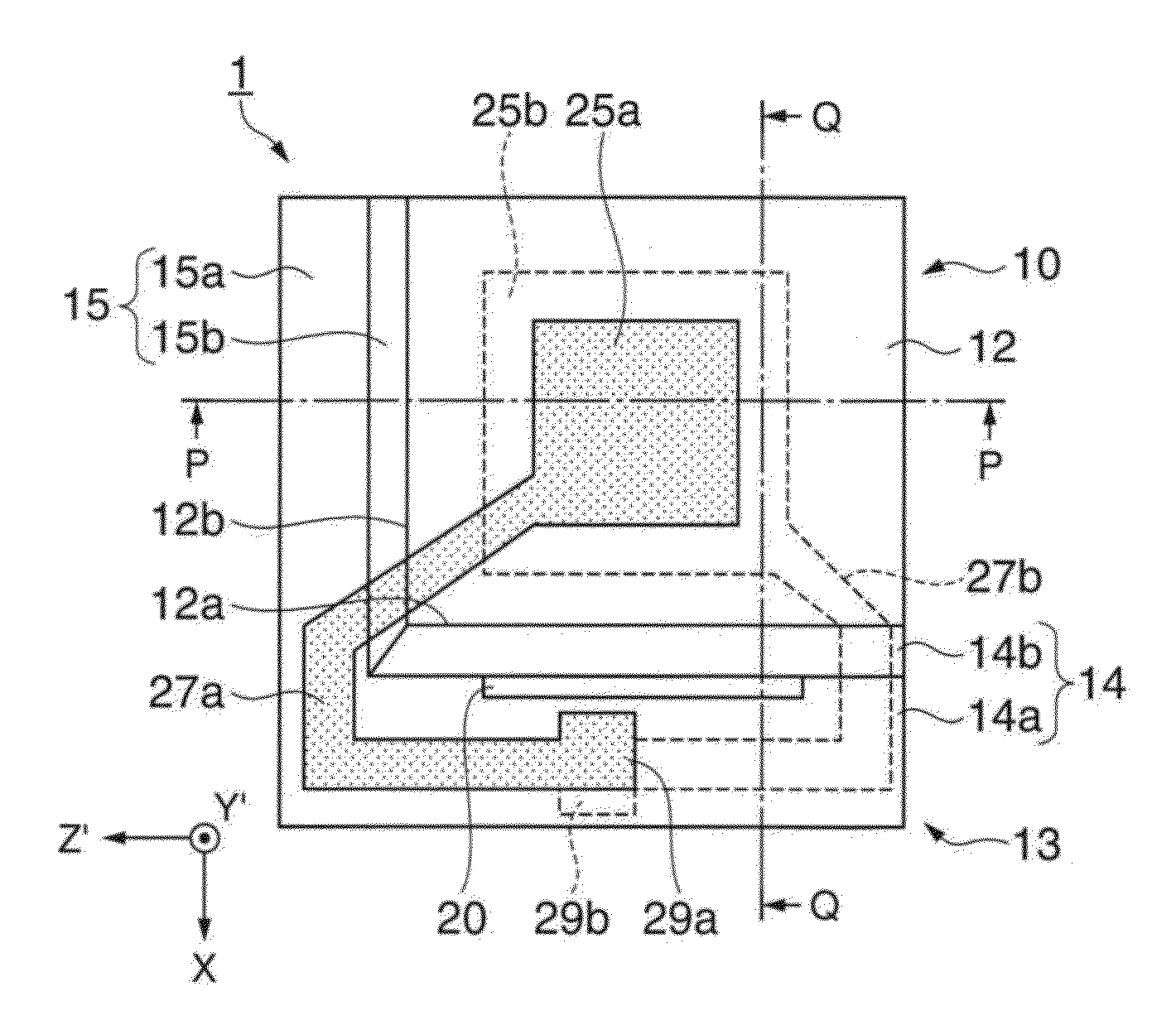
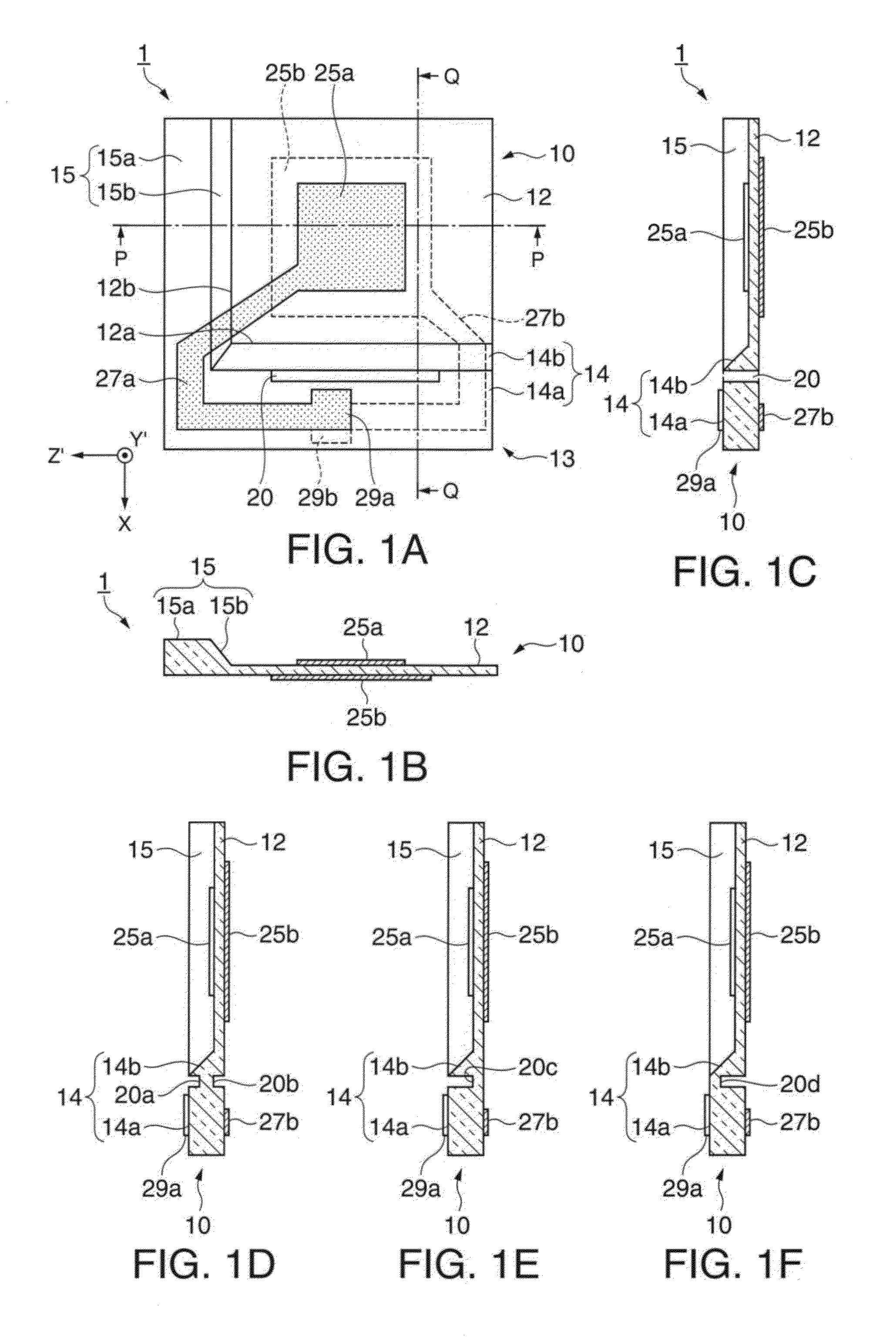
[0084]FIGS. 1A to 1F are schematic diagrams showing a configuration of a piezoelectric vibrating element 1 according to a first embodiment of the invention. FIG. 1A is a plan view of the piezoelectric vibrating element 1, FIG. 1B is a cross-sectional view of cross-section P-P taken from the +X-axis direction, FIG. 1C is a cross-sectional view of cross-section Q-Q taken from the −Z′-axis direction, FIGS. 1D, 1E, and 1F are cross-sectional view of cross-section Q-Q showing modification examples of a slit shape.

[0085]The piezoelectric vibrating element 1 includes a vibrating section 12 that includes a thin rectangular vibration area, a piezoelectric substrate 10 that is formed integrally with the vibrating section 12 and has a thick section 13 of which the thickness is greater than that of the vibration area, excitation electrodes 25a and 25b that are respectively disposed on the front and rear surfaces of the vibration area so as to oppose each other, and lead electrodes 27a and 27b t...

second embodiment

[0138]FIGS. 6A to 6C are schematic diagrams showing a configuration of a piezoelectric vibrating element 2 according to a second embodiment. FIG. 6A is a plan view of the piezoelectric vibrating element 2, FIG. 6B is across-sectional view of cross-section P-P taken from the +X-axis direction and FIG. 6C is a cross-sectional view of cross-section Q-Q taken from the −Z′-axis direction.

[0139]A difference of the piezoelectric vibrating element 2 from the piezoelectric vibrating element 1 shown in FIGS. 1A to 1F is the position where the slit 20 for easing stress is provided. In the present embodiment, the slit 20 is formed within the first inclined section 14b as being separated from the circumferential edge of the side 12a of the thin vibrating section 12. The slit 20 is not formed within the first inclined section 14b so that one circumferential edge of the slit 20 comes into contact with the side 12a along the side 12a of the vibrating section 12, but provided being separated from bo...

third embodiment

[0141]FIGS. 7A to 7C are schematic diagrams showing a configuration of a piezoelectric vibrating element 3 according to a third embodiment. FIG. 7A is a plan view of the piezoelectric vibrating element 3, FIG. 7B is across-sectional view of cross-section P-P taken from the +X-axis direction, and FIG. 7C is a cross-sectional view of cross-section Q-Q taken from the −Z′-axis direction.

[0142]A difference of the piezoelectric vibrating element 3 from the piezoelectric vibrating element 1 shown in FIGS. 1A to 1F is that two slits for easing stress are provided such that a first slit 20e is provided within a plane of the first thick section main body 14a and a second slit 20f is formed within a plane of the first inclined section 14b. The purpose of providing respective individual slits within the planes of the first thick section main body 14a and the first inclined section 14b is that, by providing two slits within the first thick section 14, expansion of stress arising during hardening...


PUM


Abstract

A piezoelectric resonating element includes a piezoelectric substrate that includes a rectangular vibrating section and a thick section integrally formed with the vibrating section, excitation electrodes, and lead electrodes. The thick section includes a first thick section and a second thick section of which one end is formed continuous to the first thick section. The first thick section includes a first inclined section of which the thickness changes and a first thick section main body of a quadrangle column shape, and at least one slit is provided in the first thick section.

Description

BACKGROUND[0001]1. Technical Field[0002]The present invention relates to a resonator having a thickness shear vibration mode as the main vibration, and particularly to a vibrating element having a so-called inverted mesa structure, a resonator, and an electronic device, an electronic apparatus, and a mobile object using such a resonator.[0003]2. Related Art[0004]An AT cut quartz crystal resonator is a resonator in which the main vibration mode which is excited is a thickness shear vibration, and since it is appropriate for miniaturization and increases in frequency, and presents a cubic curve with an excellent frequency-temperature characteristic, it has a wide variety of applications in piezoelectric oscillators and electronic apparatuses.[0005]JP-A-2004-165743 (patent literature 1) discloses an AT cut quartz crystal resonator of a so-called inverted mesa structure that includes a recess on a portion of the main plane and is designed to achieve high frequency. The length of the Z′-...

Claims


Application Information

Patent Timeline
Patent Type & Authority Applications(United States)
IPC IPC(8): H01L41/04H03B5/36
CPCH03H9/0542H03H9/0552H03H9/1021H01L41/08H03H9/19H01L41/04H03H9/131H03B5/32H03H9/172H10N30/00H10N30/80H10N30/88H10N30/2023H10N30/2042
Inventor ISHII, OSAMU
Owner SEIKO EPSON CORP
Why Eureka
Try Eureka