Group iii nitride semiconductor light emitting device

Active Publication Date: 2013-02-28
SUMITOMO ELECTRIC IND LTD +1
View PDF3 Cites 11 Cited by
  • Summary
  • Abstract
  • Description
  • Claims
  • Application Information

AI Technical Summary

Benefits of technology

[0008]The inventors have some knowledge that in a group III nitride semiconductor laser device having a pad electrode the side of which extending to the edge of an end face of an optical cavity, abnormal growth of a dielectric material may occur at the side of the pad electrode in the formatio

Problems solved by technology

But, as described above, abnormal growth of the dielectric material, however, may occur at the side of the pad electrode extending to the end face.
In addition, since the end faces of an optical cavity a

Method used


Image

  • Group iii nitride semiconductor light emitting device
  • Group iii nitride semiconductor light emitting device
  • Group iii nitride semiconductor light emitting device

Examples


example 1

[0097]A GaN substrate having a semi-polar surface is prepared and the perpendicularity nature of the fractured face is observed, as described below. A (20-21)-plane GaN substrate is used that is cut out from a thick (0001) GaN ingot grown by HVPE at an angle of 75 degrees toward the m-axis direction away therefrom. The primary surface of the GaN substrate is mirror finished, and the back surface is polished into a pearskin finish. A scribed line is formed on the pearskin back side with a diamond pen in a direction orthogonal to the c-axis projected onto the primary surface of the substrate, and then the substrate is fractured by pressing. The substrate is observed from the direction of the a-plane with a scanning electronic microscope in order to estimate the perpendicularity of the fractured face that has been formed, and this observation has shown that the fractured face has flatness and perpendicularity with respect to the semi-polar primary surface.

example 2

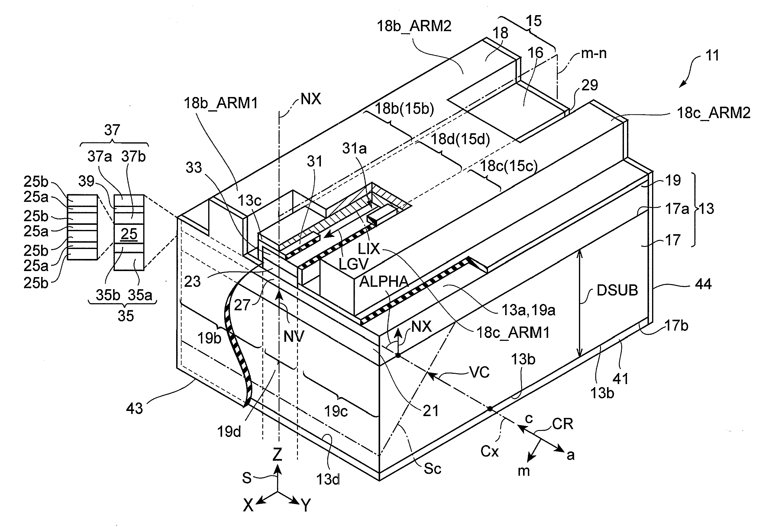
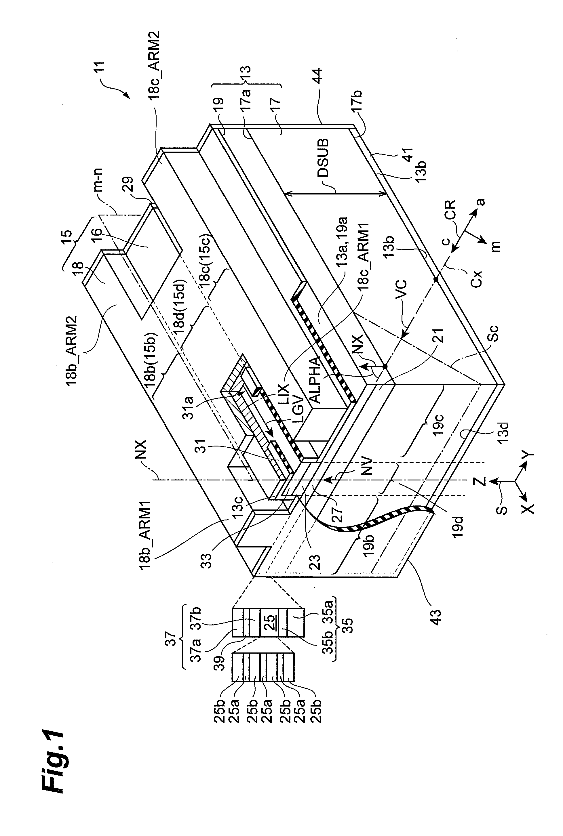
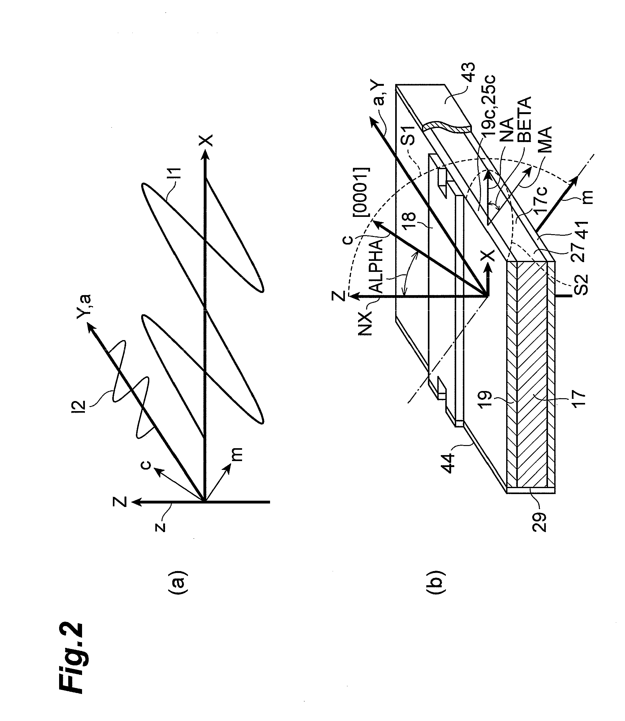
[0098]Example 1 has shown that, in the GaN substrate having a semi-polar (20-21) plane, the fractured surface obtained by pressing after forming a scribe line orthogonal to the projected c-axis on the primary surface of the substrate has flatness and perpendicularity relative to the primary surface of the substrate. In order to show the usefulness of the fractured face as a laser cavity, a laser diode which is illustrated in FIG. 7 is grown by metal organic chemical vapor deposition. The raw materials used include trimethyl gallium (TMGa), trimethyl aluminum (TMAl), trimethyl indium (TMIn), ammonium (NH3), and silane (SiH4). A substrate 71 is prepared. The substrate 71 is cut out with a wafer slicing apparatus from a thick (0001) GaN ingot grown by HVPE at an angle in the range of zero to 90 degrees formed toward the m-axis direction, so that the GaN substrate that has an inclination angle ALPHA of the c-axis formed toward the m-axis at a desired off-angle in the range of zero to 90...

example 3

[0109]An epitaxial substrate is fabricated by the procedure described in Example 2, and then, a p-side electrode and an n-side electrode are formed thereon. Two different structures (A) and (B) are prepared for the p-side electrode. Similar to the structure described in the embodiment, structure (A) includes a pad electrode having two arms (hereinafter referred to as “notched structure”). Structure (B) includes a pad electrode the entire edges of which extend along end faces of a cavity (hereinafter referred to as “notchless structure”). Dielectric multilayers of Al2O3 / TiO2 are grown on the end faces of the pad electrodes in structures (A) and (B). The reflectance of one end face is 90%, and the reflectance of the other end face is 80%. Part (a) of FIG. 9 illustrates a scanning electronic microscope image of a dielectric multilayer grown over a fractured face of a pad electrode in structure (A). Part (b) of FIG. 9 illustrates a scanning electronic microscope image of a dielectric mu...


PUM


Abstract

A group III nitride semiconductor laser device includes a laser structure, an insulating layer, an electrode and dielectric multilayers. The laser structure includes a semiconductor region on a semi-polar primary surface of a hexagonal group III nitride semiconductor support base. The dielectric multilayers are on first and second end-faces for the laser cavity. The c-axis of the group III nitride tilts by an angle ALPHA from the normal axis of the primary surface in the waveguide axis direction from the first end-face to the second end-faces. A pad electrode has first to third portions provided on the first to third regions of the semiconductor regions, respectively. An ohmic electrode is in contact with the third region through an opening of the insulating layer. The first portion has a first arm, which extends to the first end-face edge. The third portion is away from the first end-face edge.

Description

BACKGROUND OF THE INVENTION[0001]1. Field of the Invention[0002]The present invention relates to a group III nitride semiconductor laser device.[0003]2. Related Background Art[0004]Patent Literature 1 discloses a nitride-based semiconductor laser device. The semiconductor laser device in Patent Literature 1 enables the easy detection of defects caused in the device by cleaving without an increased number of steps in the manufacturing process. The nitride-based semiconductor laser device includes nitride-based semiconductor layers formed on a c-plane n-type GaN substrate, a light-emitting face of a fractured face, and p-side pad electrode formed on the nitride-based semiconductor layers. The p-side pad electrode includes a notch formed so as not to cover a ridge at the end section in which the light-emitting face 30a is located. The p-side pad electrode is disposed away from the edge of the light-emitting face.[0005]Patent Literature 2 discloses a nitride-based semiconductor laser de...

Claims


Application Information

Patent Timeline
IPC IPC(8): H01S5/30
CPCH01S5/0202H01S5/028H01S5/0425B82Y20/00H01S5/3202H01S5/34333H01S5/22H01S5/320275H01S5/04254
Inventor SUMITOMO, TAKAMICHIKYONO, TAKASHIUENO, MASAKIYOSHIZUMI, YUSUKEENYA, YOHEIADACHI, MASAHIROTAKAGI, SHIMPEIYANASHIMA, KATSUNORI
Owner SUMITOMO ELECTRIC IND LTD
Why Eureka
Try Eureka