Thin Interdigitated Backside Contact Solar Cell and Manufacturing Process Thereof

a solar cell and backside technology, applied in the field of solar cell manufacturing, can solve the problems of increasing materials costs, increasing materials costs, and inability to meet the requirements of a large number of processing steps, and achieves the effects of reducing the cost of pv cell manufacturing, high materials quality, and better control of dopant profiles

Inactive Publication Date: 2013-03-14
CRYSTAL SOLAR INC
View PDF8 Cites 5 Cited by
  • Summary
  • Abstract
  • Description
  • Claims
  • Application Information

AI Technical Summary

Benefits of technology

[0018]One aspect of the invention includes epitaxial deposition of many or all of the semiconductor layers of the solar cell on a porous layer of a mother wafer and subsequent exfoliation of the epitaxial layer, thereby reducing use of silicon compared with the conventional thick wafer process. The epitaxial deposition on porous silicon for the formation of very thin silicon wafers also avoids the multiple energy-intensive steps characteristic of the conventional process of slicing a thick solar cell wafer from an ingot. The in situ formation of P+-P and N+-P junctions during epitaxial deposition processes also provides improved control of dopant profiles within the PV cell.
[0021]The invention allows processing with a limited number of steps, which is a substantial reduction in the number of processing steps compared with the prior art furnace diffusion fabrication method, thereby lowering manufacturing costs.
[0023]Within an embodiment of the present invention, it is possible to employ epitaxial deposition to grow the necessary P- and N-type layers on top of a porous layer. It is well-known that the growth of films using epitaxial deposition affords high materials quality as compared with the conventional method of manufacturing layers in silicon wafers by furnace diffusion. In addition, with the formation of P-N junctions during epitaxial deposition, the possibility exists for much better control of dopant profiles when compared with dopant profiles generated using conventional furnace diffusion. This increased control arises from the epitaxial growth process allowing control of dopant concentrations in the material as it is deposited. This control is accomplished by the regulation and variation of the various feed gases during the epitaxial deposition process. Dopant profiles created in the bulk material by means of furnace diffusion, in contrast, are limited by the characteristics of thermal diffusion. In addition, at the surface, the formation of precipitates of the dopant species (e.g. phosphorus) may also occur, creating an undesirable layer which can cause loss of light-generated electrons near the surface of the solar cell. Thus, the use of epitaxial deposition for the growth of the necessary P- and N-type regions in the PV cell structure of the present invention affords many advantages over prior art PV cells structures fabricated using furnace diffusion.
[0025]Another aspect of the present invention allows the advantageous use of autodoping to diffuse a dopant such as up from a thicker heavily doped mother wafer through the porous layer, and then up into the portion of the wafer destined to form the thin PV cell, is used to create a heavily doped front layer used to reflect electrons back towards the backside contacts.
[0026]Because the doping for the electron reflecting layer (which will be at the front of the completed PV cell) is accomplished simultaneously with the epitaxial growth the high temperatures employed for epitaxial deposition may cause a simultaneous diffusion process within the wafer called “autodoping”. Thereby, all separate processing steps required in the prior art fabrication process to create the electron reflecting layer may be eliminated, reducing the costs of PV cell manufacture.

Problems solved by technology

A disadvantage of this type of PV cell is the inevitable partial blockage of light entering the PV cell due to the front-side connections.
A disadvantage of this prior art PV cell fabrication process is the need for thick wafers and the resulting use of substantial amounts of silicon in the completed PV cell, raising materials costs.
Another disadvantage of this prior art PV cell fabrication process is the need for a large number of processing steps: (1) at least six steps to create the P+ regions 2002, (2) at least six steps to create the N+ regions 2012, (3) two steps to create the textured N+ region 2020, (4) a step to grow or deposit the oxide passivation layer 2022, and (5) a step to deposit the anti-reflective coating 2024.
A still further disadvantage of the use of furnace diffusion in the formation of the P+ regions 2002, and the two N+ regions 2012, 2020 is the relative lack of control over the dopant profiles (boron or aluminum for P+, and phosphorus for N+) as a function of depth into the wafer 2000 within the P+ and N+ regions 2002, 2012, and 2022.
This lack of control is inherent in the furnace diffusion process, which relies on the thermal diffusion of dopants at high temperatures through the silicon lattice.
In these areas, deleterious effects on the PV cell performance can result induced by excessive electron-hole recombination.
This method is expensive due to the need for high voltage implantation.
Such thin wafer processing can be extremely difficult with high breakage and damage rates and costly handling methods.

Method used


Image

  • Thin Interdigitated Backside Contact Solar Cell and Manufacturing Process Thereof
  • Thin Interdigitated Backside Contact Solar Cell and Manufacturing Process Thereof
  • Thin Interdigitated Backside Contact Solar Cell and Manufacturing Process Thereof

Examples


Embodiment Construction

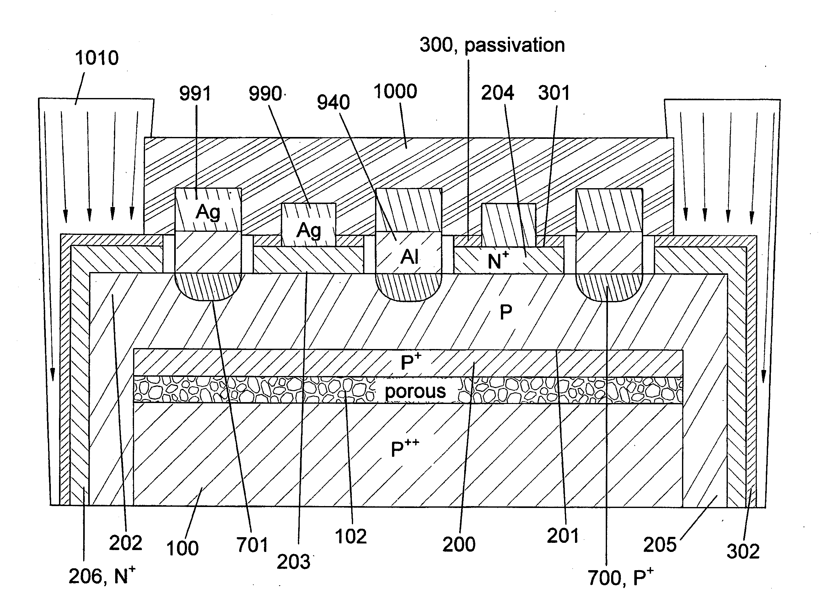
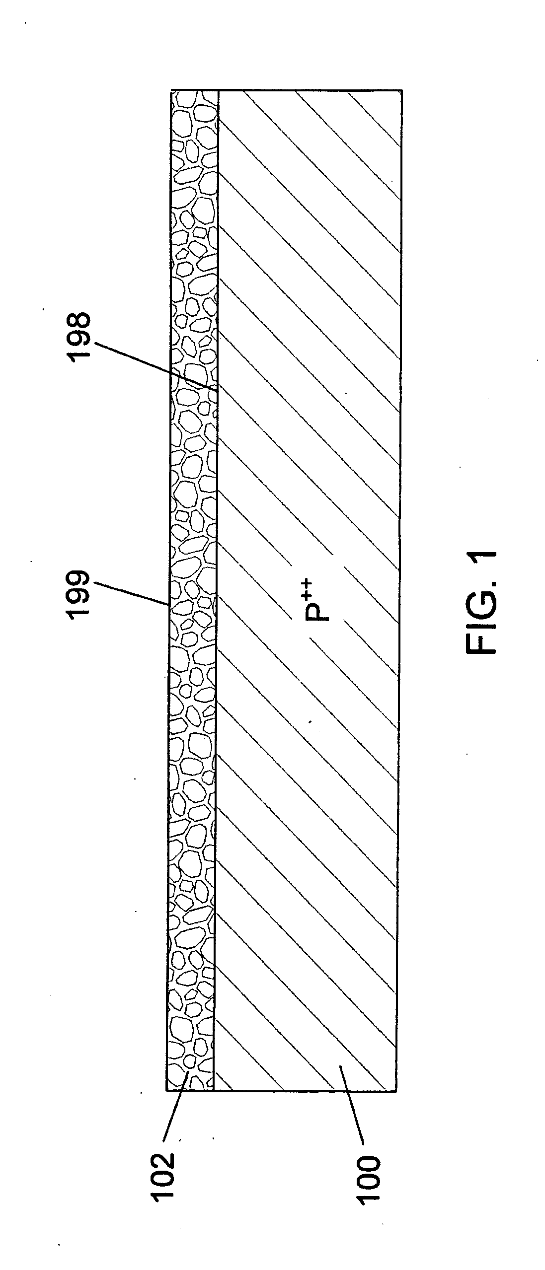
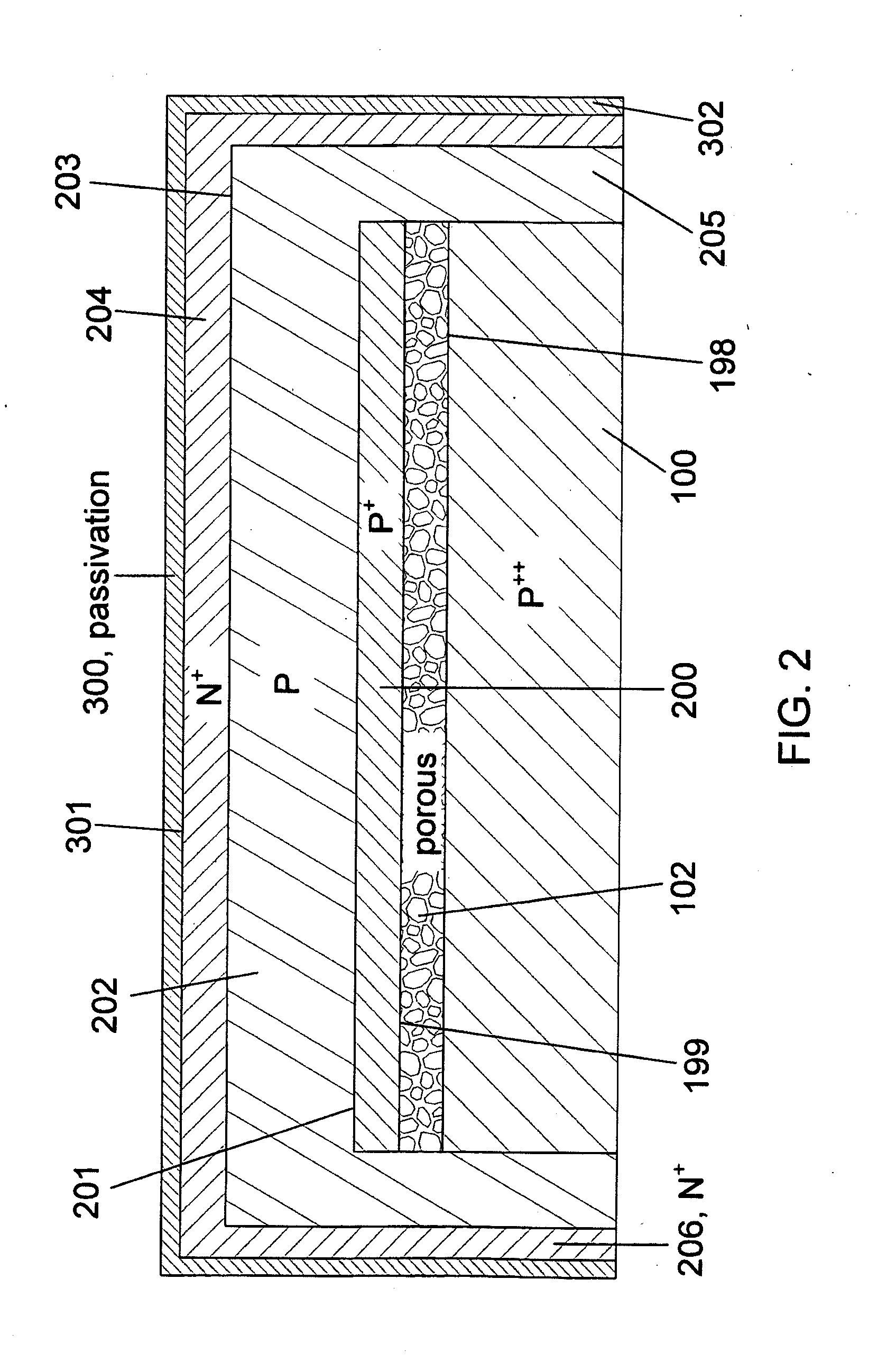
[0052]FIGS. 1 to 28 illustrate the steps in one embodiment of the fabrication process for a thin photovoltaic cell having interdigitated backside connections. Most figures are schematic side cross-sectional views in which the vertical dimensions are greatly enlarged relative to the horizontal dimensions. Note that this lack of scaling makes the profiles of the isotropic etch steps appear as vertical lines, since any undercutting occurring during the etch process cannot be seen when the vertical scale is greatly enlarged.

[0053]FIG. 1 is a schematic side cross-sectional view of a silicon wafer 100 with a thin porous silicon layer 102 at its upper principal surface. The wafer 100 may typically be P++ boron-doped silicon with a resistivity in the range 0.01 to 0.005 ohm-cm. The tipper portion of the wafer 100 is made porous by using an anodic etching process, for example, using hydrofluoric acid (HF) as the electrolyte, as described in FIG. 9 of U.S. Provisional Patent Application Ser. ...


PUM

PropertyMeasurementUnit
thicknessaaaaaaaaaa
thicknessesaaaaaaaaaa
thickaaaaaaaaaa

Abstract

A design and manufacturing method for an interdigitated backside contact photovoltaic (PV) solar cell less than 100 μm thick are disclosed. A porous silicon layer is formed on a wafer substrate. Portions of the PV cell are then formed using diffusion, epitaxy and autodoping from the substrate. All backside processing of the solar cell (junctions, passivation layer, metal contacts to the N+ and P+ regions) is performed while the thin epitaxial layer is attached to the porous layer and substrate. After backside processing, the wafer is clamped and exfoliated. The front of the PV cell is completed from the region of the wafer near the exfoliation fracture layer, with subsequent removal of the porous layer, texturing, passivation and deposition of an antireflective coating. During manufacturing, the cell is always supported by either the bulk wafer or a wafer chuck, with no processing of bare thin PV cells.

Description

CROSS-REFERENCE TO RELATED APPLICATIONS[0001]This application claims the benefit of U.S. Provisional Application Ser. No. 61 / 068,629, filed Mar. 8, 2008, which is expressly incorporated by reference herein.BACKGROUND OF THE INVENTION[0002]1. Field of the Invention[0003]This invention relates generally to the field of solar cell manufacturing, and more particularly to solar cells with interdigitated backside connections on very thin silicon wafers, for example, less than 50 microns in thickness[0004]2. Description of the Related Art[0005]There are two main types of photovoltaic (PV) cells used today. In the first type of PV cells, front side / back side connections are made through connecting ribbons soldered to bus bars to both the front and back of the PV cell. A disadvantage of this type of PV cell is the inevitable partial blockage of light entering the PV cell due to the front-side connections. In a second improved design for PV cells, all electrical connections to the PV cell dio...

Claims


Application Information

Patent Timeline
Patent Type & Authority Applications(United States)
IPC IPC(8): H01L31/0236
CPCH01L31/061H01L31/0682Y02E10/547H01L31/1892H01L31/1804Y02P70/50
Inventor RAVI, KRAMADHATI V.
Owner CRYSTAL SOLAR INC
Why Eureka
Try Eureka