Semiconductor device

a technology of semiconductors and transistors, applied in the direction of pulse automatic control, generator stabilization, oscillation generators, etc., can solve the problems of inability to estimate the direction of process deviation, influence on the operation of transistors, etc., to reduce the threshold voltage reduce the consumed power amount of the oscillation circuit section, and reduce the area of each mos transistor

Active Publication Date: 2013-03-21
RENESAS ELECTRONICS CORP
View PDF9 Cites 0 Cited by
  • Summary
  • Abstract
  • Description
  • Claims
  • Application Information

AI Technical Summary

Benefits of technology

[0020]According to the semiconductor device of the present invention, by using a plurality of MOS transistors, each of which is in a diode connection and which are connected in serial, a voltage is generated to drive an oscillation circuit section. At this time, the voltage generated by the plurality of MOS transistors is obtained based on a power supply voltage and a ratio of the threshold voltages of the MOS transistors. Therefore, it is possible to restrain on the area of each MOS transistor, to reduce the threshold voltage of each MOS transistor, and to reduce a consumed power amount of the oscillation circuit section.

Problems solved by technology

There is a problem that the operation of a transistor is influenced by a process deviation when the transistor is manufactured, in the oscillation circuit of Patent Literature 1.
However, in case of manufacturing a transistor, it is impossible to estimate the direction of the process deviation.

Method used


Image

  • Semiconductor device
  • Semiconductor device
  • Semiconductor device

Examples


first embodiment

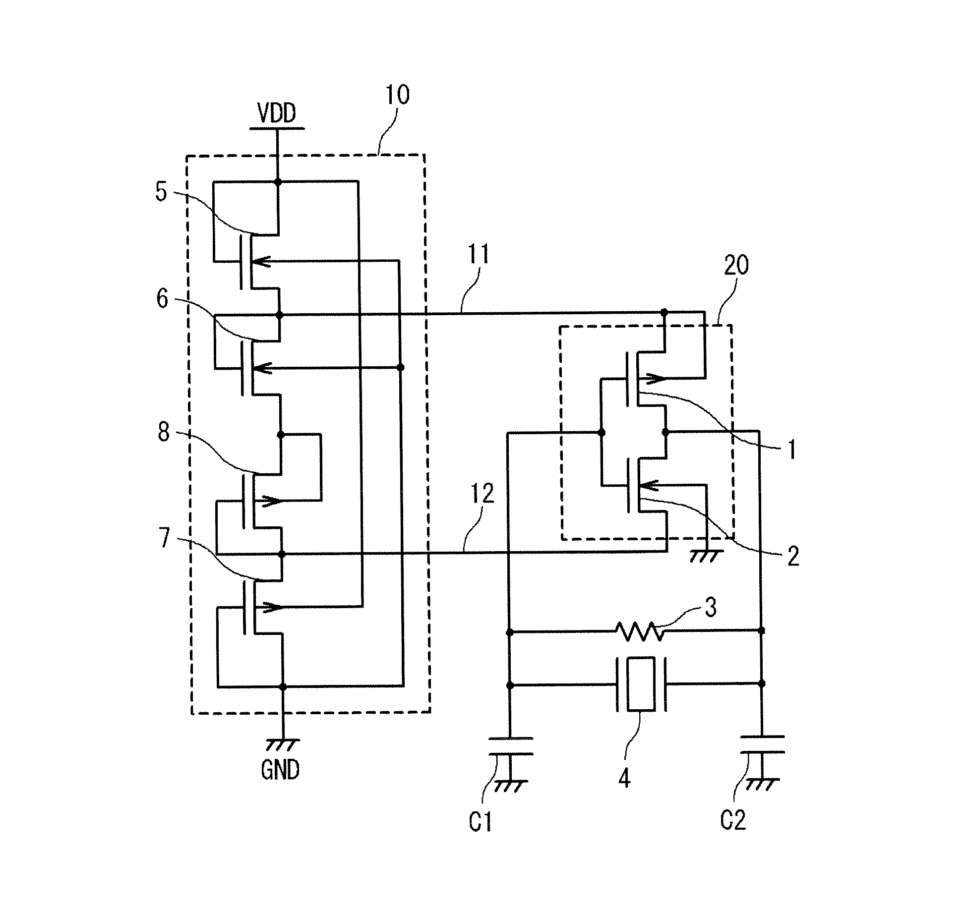
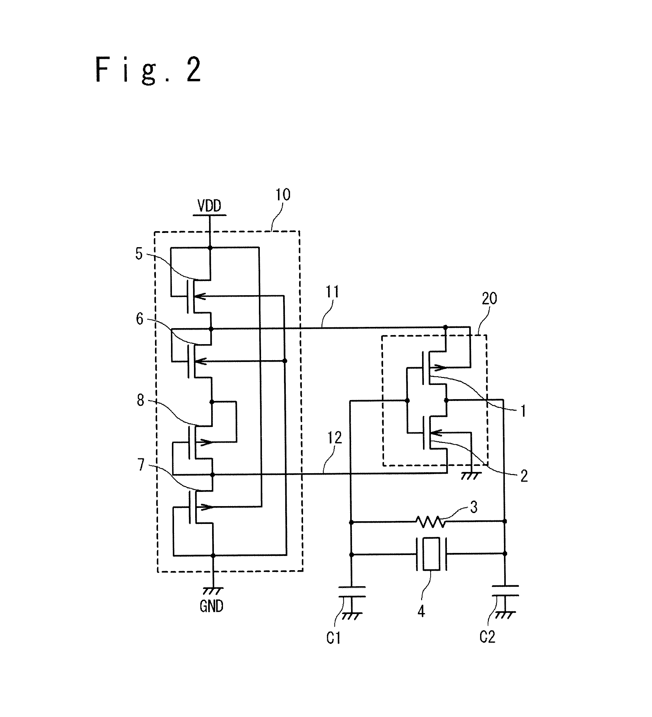
[0032]FIG. 2 is a graphic diagram showing the configuration of the semiconductor device according to a first embodiment of the present invention. Components of the semiconductor device shown in FIG. 2 will be described. The semiconductor device shown in FIG. 2 is provided with a power supply voltage VDD, a ground GND, an amplitude control circuit section 10, an oscillation gate circuit section 20, a feedback resistance 3, a resonator 4, an input side capacitor C1 and an output side capacitor C2. The amplitude control circuit section 10 is provided with first and second NMOS transistors 5 and 6, and first and second PMOS transistors 7 and 8. The oscillation gate circuit section 20 is provided with a PMOS transistor 1 and an NMOS transistor 2. Here, the oscillation gate circuit section 20, the feedback resistance 3, the resonator 4, the input side capacitor C1 and the output side capacitor C2 may be collectively referred to as an oscillation circuit section.

[0033]The connection relati...

second embodiment

[0062]FIG. 6 is a diagram showing the configuration of the semiconductor device according to a second embodiment of the present invention. The semiconductor device in the present embodiment is attained by applying the following modifications to the semiconductor device according to the first embodiment of the present invention shown in FIG. 2. That is, in the semiconductor device of FIG. 2, the back gate of the second PMOS transistor 8 is connected with the source of the second PMOS transistor 8 and the source of the second NMOS transistor 6 in common. Also, in the semiconductor device of FIG. 2, the back gate of the second NMOS transistor 6 is grounded. However, in the semiconductor device of the present embodiment, the back gate of the second NMOS transistor 6 is connected with the source of the second PMOS transistor 8 and the source of the second NMOS transistor 6 in common. Also, in the semiconductor device of the present embodiment, the back gate of the second PMOS transistor ...

third embodiment

[0066]FIG. 7 is a circuit diagram showing the configuration of the semiconductor device according to a third embodiment of the present invention. The semiconductor device of FIG. 7 is attained by applying the following modifications to the semiconductor device according to the first embodiment of the present invention shown in FIG. 2. That is, a control circuit section 36 and a selector circuit section 40 are added.

[0067]An amplification factor of the oscillation circuit in which the circuit configuration containing a transistor size has been determined, changes according to the current flowing through the oscillation circuit (or, the voltage applied to the oscillation circuit). Generally, in the oscillation circuit, the amplification factor which is required to start the oscillation is higher than the amplification factor which is required to sustain the oscillation. In other words, when the current which flows through the oscillation gate circuit section 20 (or, the voltage which ...


PUM


Abstract

An oscillation circuit section is provided which can attain the reduction of a consumed power amount and the reduction of a manufacturing cost. In a semiconductor device, voltages are generated to drive the oscillation circuit section by using a plurality of MOS transistors which are connected in serial and each of which is in a diode connection. At this time, each voltage is generated based on a power supply voltage and a ratio of the threshold voltages of the plurality of MOS transistors. Therefore, it is possible to suppress the threshold voltage of each MOS transistor, to save an area of each MOS transistor, and to reduce the consumed power amount of the oscillation circuit section.

Description

CROSS REFERENCE[0001]This patent application claims a priority on convention based on Japanese Patent Application No. JP 2011-201303. The disclosure thereof is incorporated herein by reference.TECHNICAL FIELD[0002]The present invention is related to a semiconductor device, and especially, to a semiconductor device which has an oscillation circuit.BACKGROUND ART[0003]Miniaturization proceeds in a mobile information terminal and a DSC (Digital Still Camera) and so on. With the miniaturization of the terminal, a battery is also miniaturized, and a case where a button cell of a small capacity is used is increasing. For this reason, a low consumed power amount is required even to an oscillation circuit which always operates inside the LSI (Large Scale Integration).[0004]As a method of supplying power to such an oscillation circuit, a conventional technique is known in which a power supply voltage from a constant voltage circuit is lowered to a constant voltage, and the lowered voltage is...

Claims


Application Information

Patent Timeline
Patent Type & Authority Applications(United States)
IPC IPC(8): H03L5/00
CPCH03L5/00H03L1/00H03B5/364H03B5/04
Inventor SUZUKI, SANAE
Owner RENESAS ELECTRONICS CORP
Why Eureka
Try Eureka