
Inkjet head and method for producing the same

a technology of inkjet head and nozzle, which is applied in the direction of printed circuit, printing, non-metallic protective coating application, etc., can solve the problems of short circuit between the wirings, product malfunction, product failure, etc., and achieves excellent ion migration resistance, simple configuration, and cost reduction.

Inactive Publication Date: 2013-03-28
FUJIFILM CORP
View PDF6 Cites 14 Cited by
  • Summary
  • Abstract
  • Description
  • Claims
  • Application Information

AI Technical Summary

Benefits of technology

The present invention provides an inkjet head that is resistant to moisture and solvents, which helps prevent the migration of ions. This is achieved by adding a copper ion diffusion inhibiting film to the wiring member of the flexible wiring circuit board, which contains copper. This results in a simple and cost-effective configuration that still exhibits excellent resistance to ion migration.

Problems solved by technology

When the fluid penetrates or permeates the connection portion of the flexible wiring circuit board, ion migration occurs between the wirings during the operation, which may cause short-circuit between the wirings.
This short-circuit, being unexpected conduction, causes malfunction of a product, or at the worst, failure of the product.
Due to this structural feature, ion migration resistance is weakest at the edge, which is likely to cause the ion migration at the time of activation, resulting in the short-circuit.
The short-circuit leads to incorrect image rendering and results in a printing defect such as deterioration of image quality or failure.
Selection or development of the sealant satisfying all the above requirements takes a long time.
In a long term, the sealant is degraded by the solvent, resulting in degradation of the moisture resistance.
Thereby, corrosion of the copper wiring member caused by moisture penetration in a resin material is inhibited.
As for the Japanese Patent Laid-Open Publication No. 2008-126629, it is difficult to precisely affix the protective film made from the inorganic material to the protective layer.
A liquid permeates from the uncovered area, which degrades the ion migration resistance.
However, when the edge of the protective layer is completely covered with the protective film, the protective film may interfere with the wiring circuit board of the die due to the structure.
This obstructs the connection of the electrical connection portion.
Accordingly, the production steps are complicated and burdensome and increase cost.

Method used


Image

  • Inkjet head and method for producing the same
  • Inkjet head and method for producing the same
  • Inkjet head and method for producing the same

Examples


Embodiment Construction

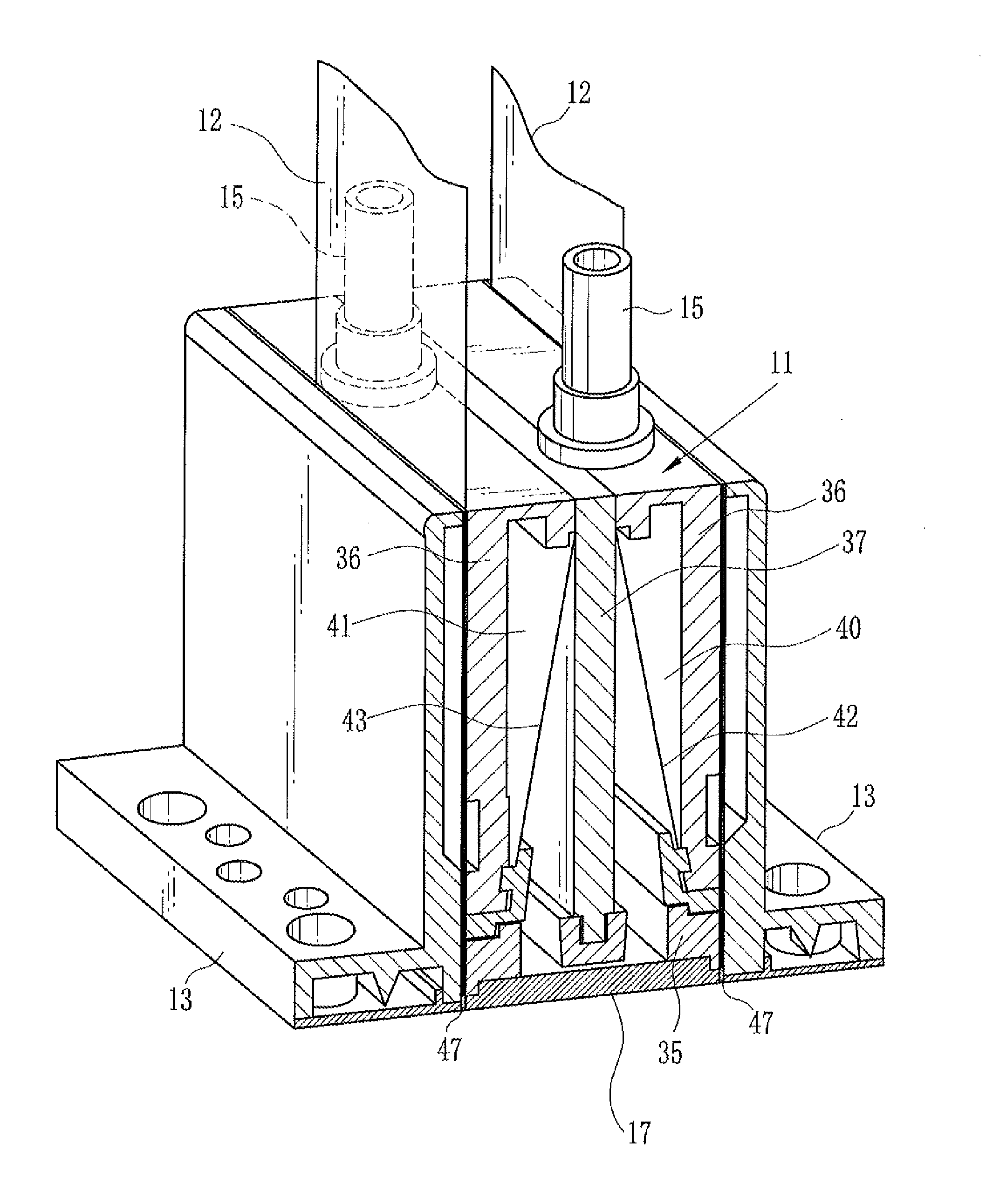
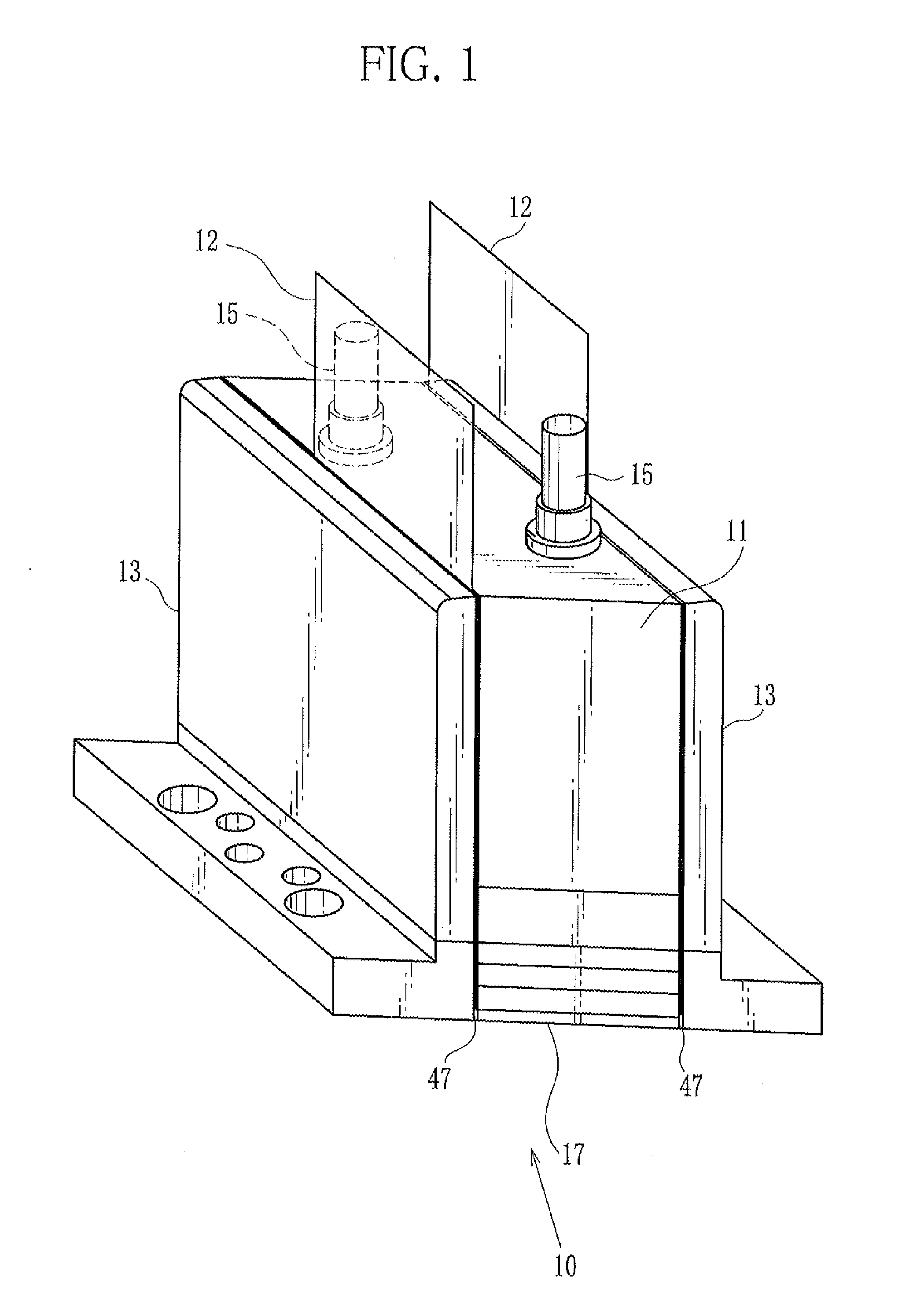
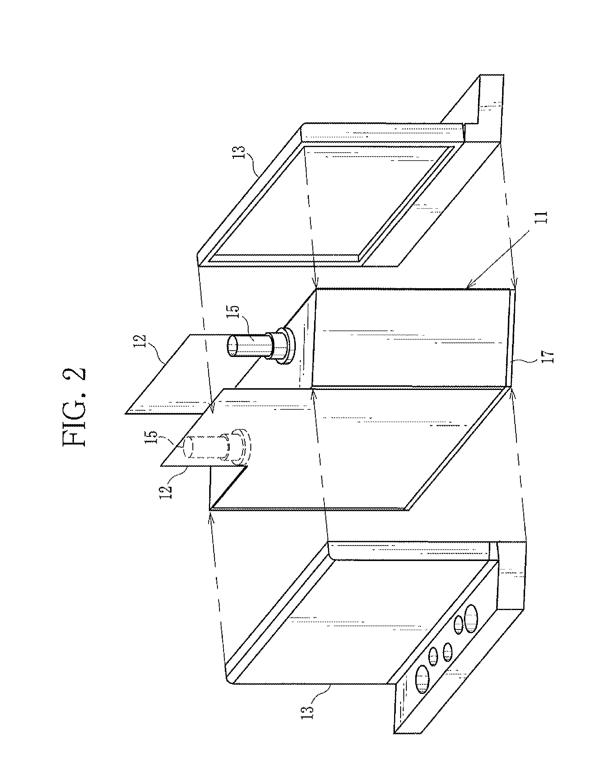
[0046]In FIG. 1, an inkjet head 10 is composed of a head body 11, a pair of flexible wiring circuit boards 12, and a pair of mounting frames 13. In FIG. 2, the head body 11 has a rectangular parallel-piped shape. Two tube connection nozzles 15 are provided on a top face of the head body 11. A discharge die 17 is provided on a bottom face of the head body 11. One of the tube connection nozzles 15 is for supplying ink and the other is for recovering the ink. When the inkjet head 10 is installed in an inkjet printer (not shown), an ink tube from an ink supply tank (not shown) is connected to the tube connection nozzle 15 for supplying the ink and an ink tube from an ink recovery tank (not shown) is connected to the tube connection nozzle 15 for recovering the ink.

[0047]On each side of the head body 11, the flexible wiring circuit board 12 is attached. To protect the flexible wiring circuit boards 12, the mounting frame 13 is adhered to each flexible wiring circuit board 12 using a two-...


PUM


Abstract

A flexible wiring circuit board has a second terminal section bonded and electrically connected to a first terminal section of a wiring circuit board of a discharge die. A drive signal is inputted to the first terminal section through the second terminal section, and then sent to a driver IC. The driver IC drives a piezoelectric element in accordance with the drive signal through a printed wiring pattern. Thereby, ink is discharged from an ink discharge opening. A copper ion diffusion inhibiting film is formed on a surface of a copper wiring member of the second terminal section on contact with a process liquid containing at least one of 1, 2, 3 triazole and 1, 2, 4 triazole. This inhibits diffusion of copper ions and copper ion migration resulting therefrom. Thus, malfunction due to the copper ion migration is inhibited.

Description

BACKGROUND OF THE INVENTION[0001]1. Field of the Invention[0002]The present invention relates to an inkjet head and a method for producing the same.[0003]2. Description Related to the Prior Art[0004]Recently, development of inkjet printers has been promoted to achieve high performance. Some models of the inkjet printers are required to have high output resolution of, for example, 1200 dpi comparable to that of offset printing. To achieve the high resolution, discharge openings and actuators such as piezoelectric elements, which allow ink to be discharged, need to be implemented with high density. For example, in U.S. Pat. No. 7,052,117, a semiconductor processing technique is employed to produce a discharge die having nozzles, ink channels, pump chambers, the piezoelectric elements, and the like. Thereby, the discharge openings are implemented with high density.[0005]The ink channels are formed in the discharge die. Each ink channel has the pump chamber and the discharge opening. Th...

Claims


Application Information

Patent Timeline
IPC IPC(8): B41J2/14H01L21/02
CPCB41J2/161B41J2/1623B41J2/1643B41J2002/14362B41J2002/14491H05K3/28H05K3/285H05K2203/124H05K3/244H05K3/363H05K3/365H05K2201/0769H05K1/117H05K3/361
Inventor NOSAKA, NORIHITOWAKABAYASHI, AKIRAOGIKUBO, SHINYAHARA, MINAKO
Owner FUJIFILM CORP
Learn More